
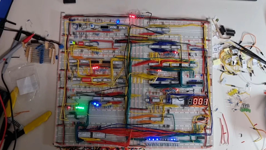
This is my build of YouTuber Ben Eater's 8-bit Breadboard Computer project. The goal was to learn how a CPU works by building one myself, starting from the lowest level.
Project Overview
This 8-bit computer implements a complete general-purpose computer using only 74LS-series TTL logic chips. There is no microcontroller or FPGA: everything is built by wiring dozens of discrete logic chips on breadboards. The finished computer handles 8-bit data and 4-bit instructions + 4-bit addresses.
A modern CPU is a black box made of billions of transistors, but this project lets you answer questions like these: How does an electrical signal perform addition? How is an instruction decoded and turned into actual operations? Why do we need a clock? What is physically different between a register and memory?
Hardware Components
The whole system is built around a shared 8-bit bus, with each module attached to it. Each module operates through control signals that either put a value onto the bus (out) or read a value from the bus (in).
1. Clock
A 555 timer IC generates the clock signal. The frequency is adjustable with a potentiometer, and the design can switch between manual mode (one cycle per button press) and automatic mode. When debugging, manual mode lets you check every control signal and the bus state by eye.
2. Registers (A, B, Instruction Register)
Two 74LS173 4-bit D flip-flop chips are connected in parallel to form an 8-bit register. Each register is controlled by these signals:
- Load: stores the bus value in the register on the rising clock edge
- Enable: drives the register value onto the bus (3-state buffer)
The IR (Instruction Register) holds the instruction: the upper 4 bits are the opcode and the lower 4 bits are the operand address.
3. ALU (Arithmetic Logic Unit)
Two 74LS283 4-bit binary adders implement 8-bit addition. Subtraction is done in two's complement: the B register value is inverted through XOR gates and carry-in is set to 1 (A - B = A + (~B) + 1).
The ALU takes the A and B registers as operands and drives the result onto the bus. It also generates the Zero and Carry flags used for conditional branches.
4. RAM (Random Access Memory)
Two 74LS189 16×4 SRAMs implement 16 bytes of RAM. There is also a programming mode for entering addresses and values by hand with DIP switches before running a program, so you can load a program directly each time.
The MAR (Memory Address Register) selects the address, and the RAM either drives the value at that address onto the bus or stores the bus value at that address.
5. Program Counter (PC)
A 74LS161 4-bit counter chip forms the 4-bit PC. It increments automatically on each clock (CE signal), and on a jump instruction it loads the bus value into the PC (J).
6. Output (Display)
A 4-digit 7-segment display shows the 8-bit value in decimal. An EEPROM (28C16) serves as a binary-to-BCD lookup table: given the 8-bit value as an address, it outputs the segment pattern for that digit. A timer switches quickly between the 4 digits to multiplex them.
7. Control Logic
This is the most complex part of the project. Two 28C256 EEPROMs act as the control signal generator. The inputs are the opcode (4 bits) + flags (2 bits) + microstep counter (3 bits), and the outputs are 16 control signals.
In other words, each instruction is broken into several microsteps, and which control signals to assert at each step is burned into the EEPROM ahead of time. I built a separate programmer with an Arduino Nano to program the EEPROMs.
Instruction Set
It supports 16 opcodes (4 bits):
| Opcode | Instruction | Operation |
|---|---|---|
| 0000 | NOP | Does nothing |
| 0001 | LDA addr | RAM[addr] → A |
| 0010 | ADD addr | A + RAM[addr] → A |
| 0011 | SUB addr | A - RAM[addr] → A |
| 0100 | STA addr | A → RAM[addr] |
| 0101 | LDI imm | imm → A |
| 0110 | JMP addr | PC ← addr |
| 0111 | JC addr | If Carry, PC ← addr |
| 1000 | JZ addr | If Zero, PC ← addr |
| 1110 | OUT | A → Display |
| 1111 | HLT | Halt |
Instruction Execution Cycle
Each instruction consists of two common fetch steps plus instruction-specific execute steps.
Fetch:
- T0: PC → MAR (next instruction address into the MAR)
- T1: RAM[MAR] → IR, PC++ (read the instruction and increment the PC)
Execute (for LDA): 3. T2: IR[3:0] → MAR (operand address) 4. T3: RAM[MAR] → A (data into A) 5. T4: (done)
All of this microcode is stored in the EEPROM control signal table, so the hardware runs it automatically.
Building It
I wired six breadboards with hundreds of jumper wires. I tested each module on its own and then integrated them one by one. Most of the debugging was hunting down wiring mistakes and faulty chips, and an oscilloscope and a logic analyzer were indispensable.
Test Program
Once it was finished, I wrote and ran a program that computes the Fibonacci sequence. It stores operands in memory and implements the loop with a combination of ADD/STA/JMP. Starting from 0 and 1, it adds them alternately and shows each value on the 7-segment display with the OUT instruction.
What I Learned
- The essence of a CPU: a CPU is ultimately a combination of a shared bus + registers + control signals, and as long as the control signal timing is right, any operation is possible
- Microcode: the design of breaking instructions into microsteps is still used in modern CISC CPUs (x86 and others)
- Clock synchronization: every signal must act on the same clock edge. Asynchronous operation leads to race conditions
- The value of debugging: even if the logic design looks right on paper, most bugs show up in the physical wiring
Through this project I got a real feel for how the fetch-decode-execute cycle, microarchitecture, and control unit design I had read about in computer architecture books are actually implemented as circuits.
 Other Project