Chapter 4: Processor Concepts and Design Overview
The processor is the brain of an SoC that executes instructions. This chapter summarizes the basic building blocks of a processor, its processing stages, instruction abstraction, the ISA, and the difference between a core and a processor.
What Is a Processor?
- HW that executes instructions to perform operations
- Required resources: registers, ALU, control unit, memory interface
Processing Stages of a Processor
- Fetch: read the instruction from memory
- Decode: interpret the instruction
- Execute: ALU operations, data processing
- Memory Access: load/store
- Write Back: store the result in a register
The Programmer's View
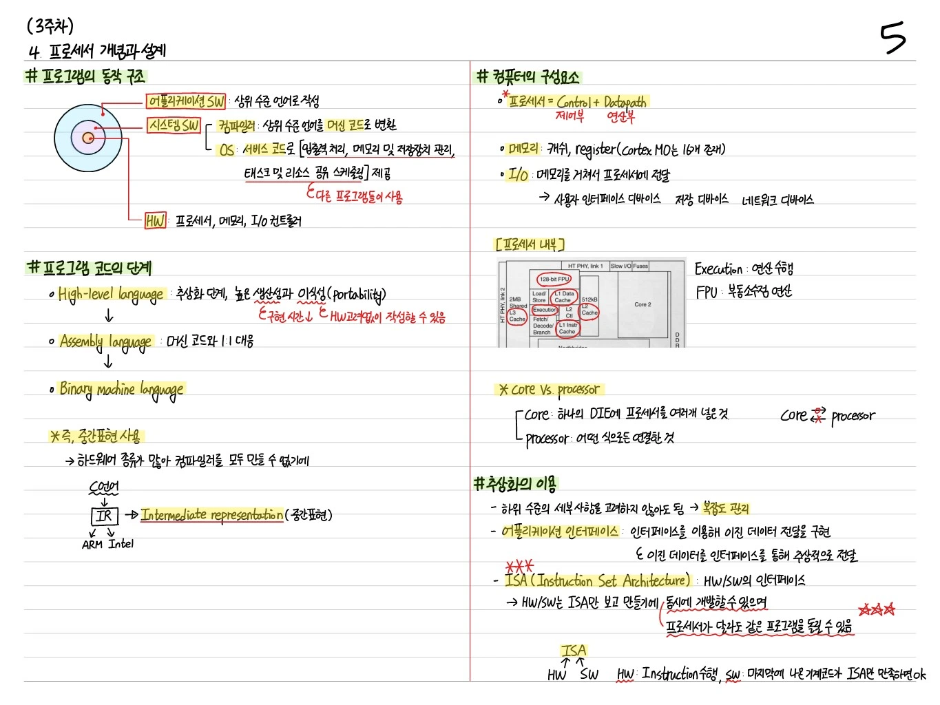
Level of Abstraction
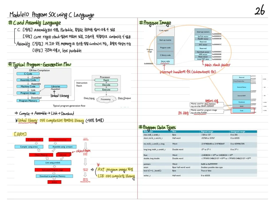
- High-level language: C, Python, Java
- Assembly language: a symbolic representation close to machine code
- Binary machine code: a stream of 0/1 bits
→ The compiler converts high-level code to assembly, and the assembler converts assembly to binary.
Core vs Processor
- Core: the central compute unit of a processor (ALU + registers + control)
- Processor: core + cache + memory controller + I/O interface
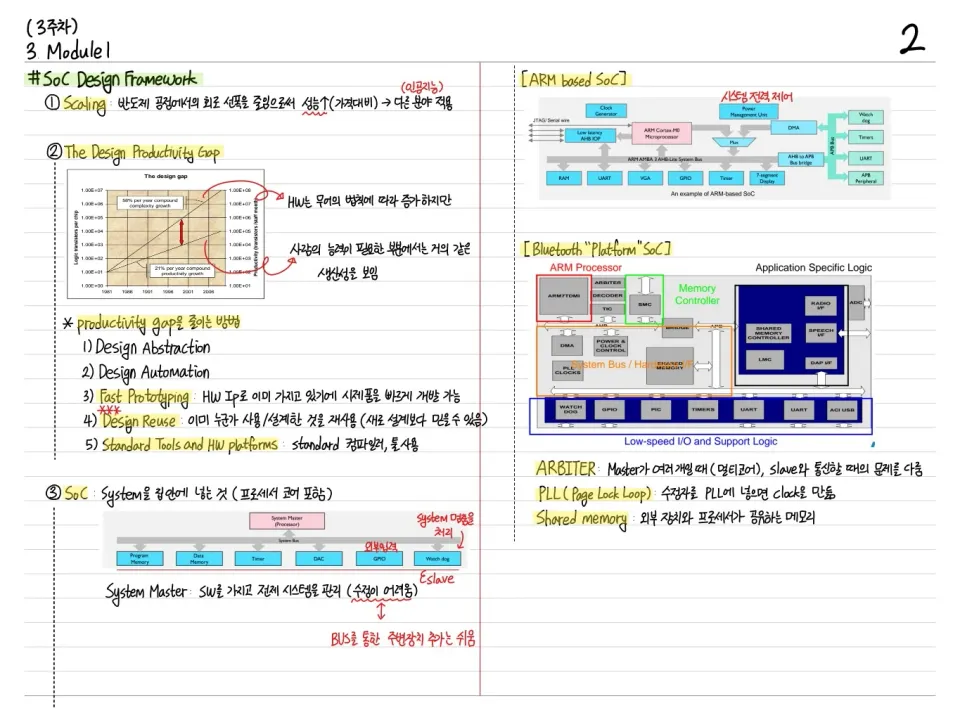
Example: a processor (SoC) such as the STM32F103 is built by licensing the ARM Cortex-M0 core. ARM designs the core, and each vendor provides the surrounding IP.
Examples of Cores
- ARM Cortex-A/R/M series
- ARM Cortex-M0/M3/M4 — Cortex-M family
Levels of Abstraction
- Microarchitecture: implementation details such as the pipeline, caches, and branch predictor
- ISA (Instruction Set Architecture): the instruction set, registers, and memory model. The interface exposed to the programmer
Several microarchitectures implement the same ISA (ARMv7-M) → Cortex-M3, M4, M7, and so on.
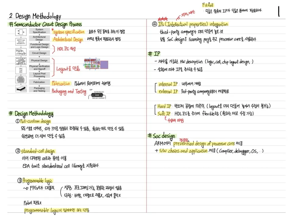
Processor Design Flow
- Choose the ISA: ARM, RISC-V, MIPS, x86, …
- Design the microarchitecture: pipeline stages, branch prediction, cache structure
- Write the RTL: implement in Verilog/VHDL
- Synthesis: convert to a gate-level netlist
- Place & Route: layout
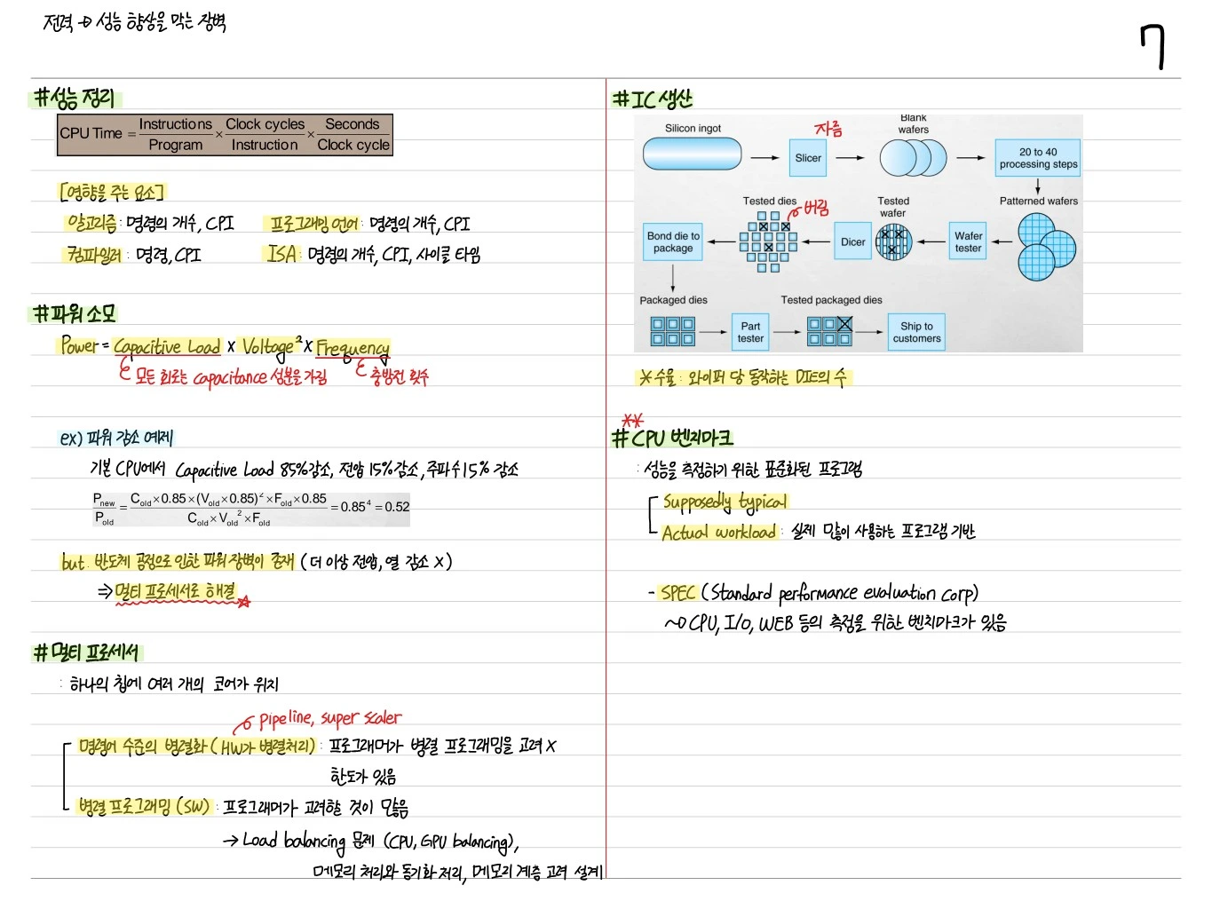
- Fab: wafer manufacturing
The ARM Cortex Family
- Cortex-A (Application): high performance, for Linux/Android (iPhone, Raspberry Pi)
- Cortex-R (Real-time): real-time, automotive/HDD (deterministic latency)
- Cortex-M (MCU): low-power MCUs (STM32, nRF52)
Cortex-M in Detail
- M0/M0+: ultra-low power, ARMv6-M (Thumb only)
- M3: ARMv7-M (Thumb-2)
- M4: M3 + DSP/FPU
- M7: high-performance MCU
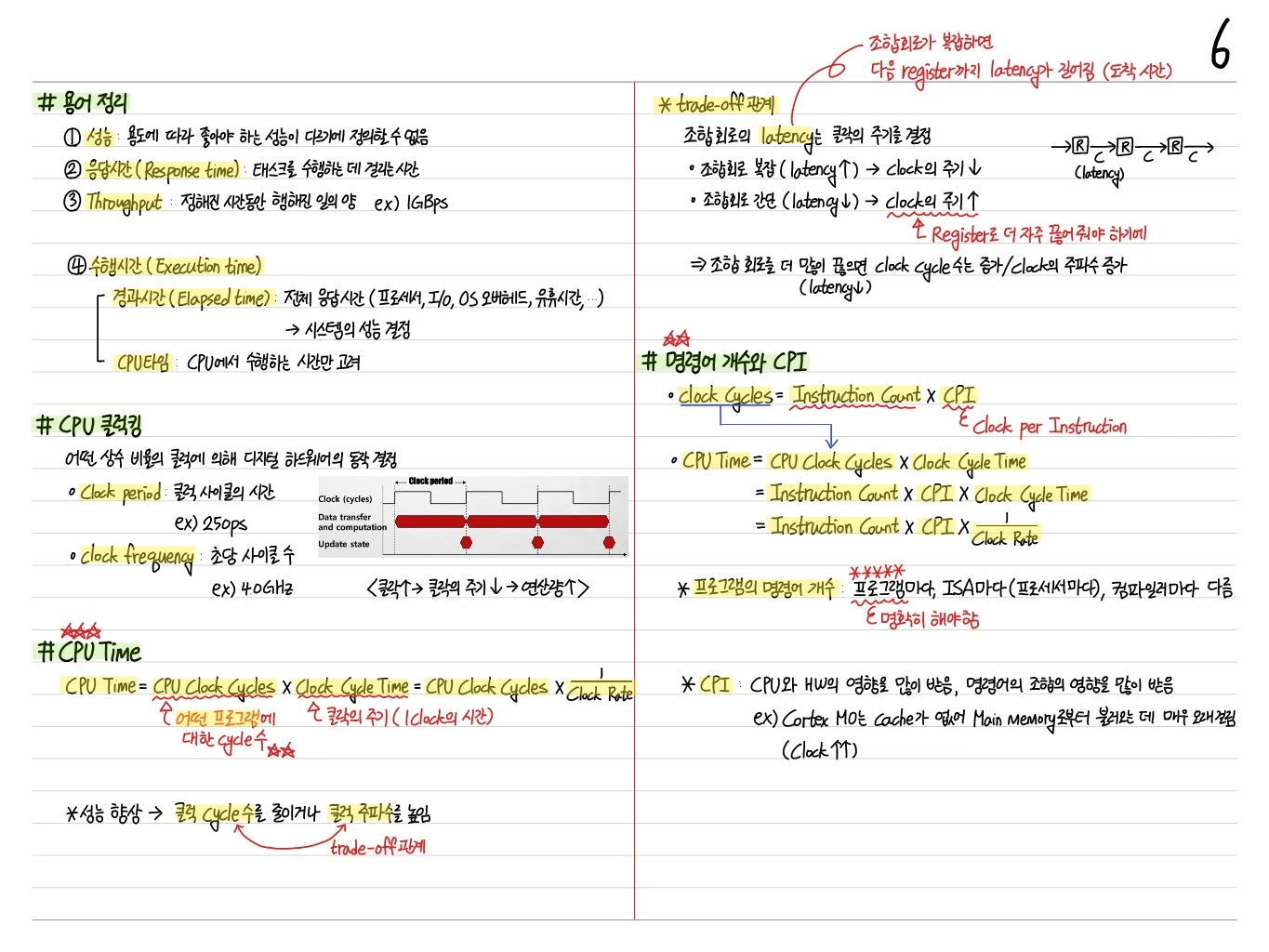
Trade-offs in Processor Design
- Performance: clock frequency, IPC (instructions per cycle)
- Power: static + dynamic
- Area: silicon area
- Verification: verification complexity
The Cortex-M0 is tiny at 11k gates → a good fit for low-cost MCUs, while the Cortex-A72 uses millions of gates for high performance → smartphone APs.
ISA Examples
- ARM: RISC, fixed-length, load/store
- Thumb/Thumb-2: compact 16-bit ARM encoding, saves code space
- x86: CISC, variable-length
- RISC-V: open-source RISC, extensible
ARM is a load/store architecture → memory is accessed only through LDR/STR, and arithmetic happens only between registers.
Example: Executing an ADD Instruction
ADD r0, r1, r2- Fetch: read the instruction binary at the PC (
0xE0810002) - Decode: interpret opcode=ADD, Rd=r0, Rn=r1, Rm=r2
- Execute: the ALU computes r1 + r2
- Write Back: store the result in r0
- PC += 4: next instruction
Summary
| Concept | Description |
|---|---|
| Processing stages | Fetch → Decode → Execute → Memory → Write-back |
| Core vs Processor | Core = ALU+Reg+Control, Processor = Core + peripherals |
| ISA | Programmer interface (ARM, x86, RISC-V) |
| Microarchitecture | How the ISA is implemented (pipeline, caches) |
| Abstraction | HLL → Assembly → Binary |
Processors evolve along two axes, the ISA and the microarchitecture, and SoC designers license the core IP they need and integrate it into the whole system.