1. Design Topic
Design an amplifier using SIMetrix
2. Design Requirements
-
Gain of 60 dB or more
-
An amplifier with a differential input and a single-ended output
-
Show the output waveform for a 1 mV, 1 kHz AC signal
-
VIN = 5 V, using 100 uA of current or less
3. Design Process
1) Designing the First Stage with a Differential Amplifier
The first stage was driven with a 1 mVpp differential input, with VIN = 5 V and 100 uA of current or less. I also used a current mirror so that the whole circuit could draw the same current reliably.
First, I built the differential amplifier as shown in Figure 1. To take a single-ended output from the differential amplifier, I added a current mirror to it.
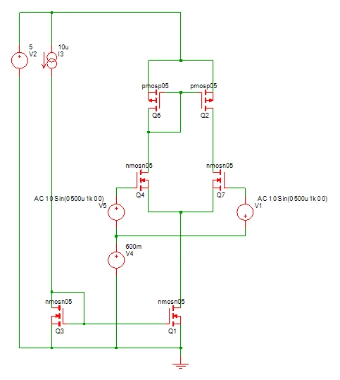
Figure 1 Differential amplifier
Next, to set the bias, I observed the output waveform while sweeping the V4 voltage. Figure 2 plots the output voltage against V4.
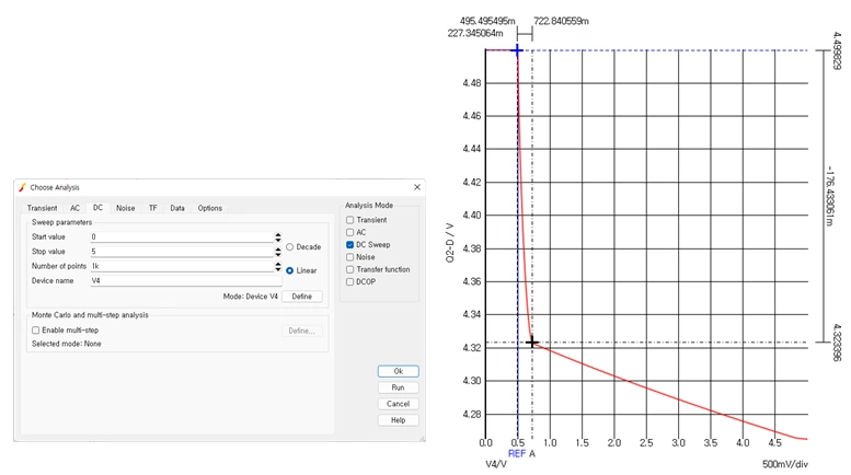
Figure 2 Output waveform while sweeping the V4 voltage
The output waveform shows the range over which the circuit can amplify. In the graph in Figure 2, that range is about 4.3 V to 4.5 V. The important point is that the DC level sits at about 4.4 V, and when this stage is later connected to the second-stage amplifier, this voltage is what biases the second amplifier. If it is too high, it may fall outside the second amplifier's bias range. So I added a resistor at the top to lower the DC voltage and a resistor at the bottom to stabilize the bias.
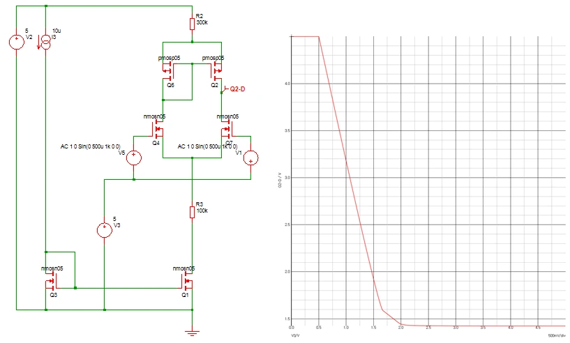
Figure 3 Output waveform while sweeping the V3 voltage (with resistors added)
Figure 3 shows the output waveform while sweeping the V3 voltage with the resistors added. The slope of the graph decreased, so the gain went down, but the input range widened, which made the bias more stable, and the output DC voltage dropped.
In this state, I set the bias point. At the midpoint, the input is 1.06 V and the output is about 3 V.
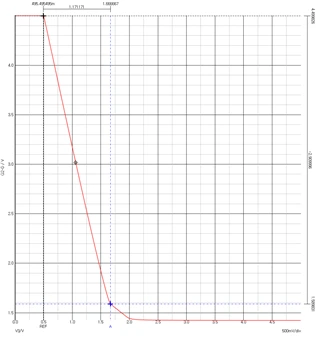
Figure 4 Setting the bias point
Figure 5 shows the completed first-stage amplifier and its output waveform. This stage gives about 42.8 dB of gain. The common-mode voltage of the differential amplifier was applied by dividing the 5 V input voltage with resistors. The design calls for about 60 dB of gain, so I added another amplifier after it to raise the gain.
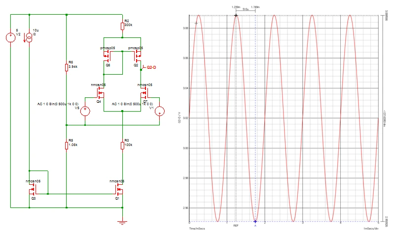
Figure 5 Completed first-stage amplifier and its output waveform
2) Designing the Second Stage with a Source-Coupled Amplifier
For the second stage, I used a source-coupled amplifier, which combines two CS stages. A CS stage needs its source tied to an AC virtual ground, which is normally done with a capacitor. However, using a source-coupled amplifier is a better way to create the virtual ground than using a capacitor, so I designed the stage as a source-coupled amplifier.
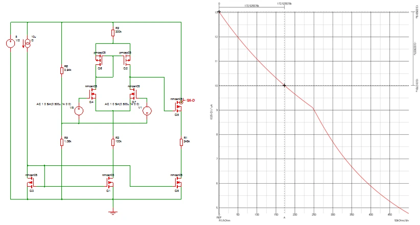
First, to set the current through the CS amplifier, I added a resistor that stabilizes the bias. I chose its value by sweeping the resistor and plotting the resulting current. Figure 6 shows this graph. I found the resistance at which 10 μA flows and got a value of about 172.5k.
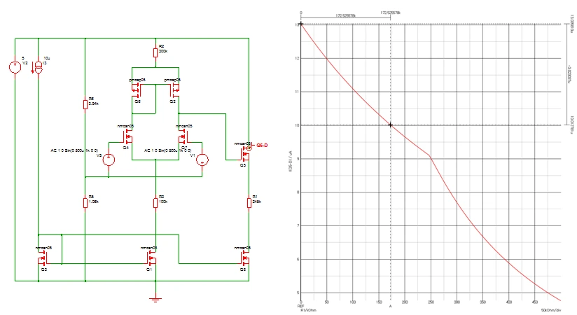
Figure 6 Current vs. resistor R1
Next, to form the output, I added a resistor above the CS stage. To choose this value as well, I swept the resistor and obtained the output voltage graph in Figure 7. I chose 200k for R8 so that the output could swing around roughly 3 V. Then I converted the CS stage into a source-coupled amplifier as shown in Figure 8. Merging the resistors into one made R1 245k.
I also applied the same input DC voltage, 3.02 V, on the right-hand side.
Up to this point, the amplifier was designed to stay within a range where it produces a stable output. But a higher output gain means a higher-performance amplifier, so I increased the output resistance as far as the waveform would go without distorting. In other words, I designed it close to the maximum voltage range it can amplify. I chose 350k for R4.
Of course, choosing values close to the maximum amplifiable range has a downside: noise can change the size of the input waveform and push it past that range, reducing stability. However, the goal of this design was to get a large gain from the amplifier, so I chose 350k for R4 to favor high gain over stability.
Figure 8 is the schematic of the completed amplifier, and its output waveform is included in the design results.
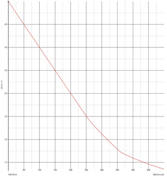
Figure 7 Current vs. resistor R8
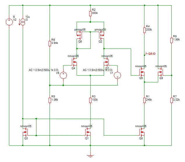
Figure 8 Final circuit design
4. Design Results
1) Input Waveform
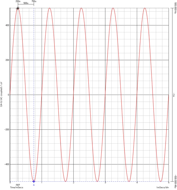
Figure 9 Input waveform
2) Output Waveform
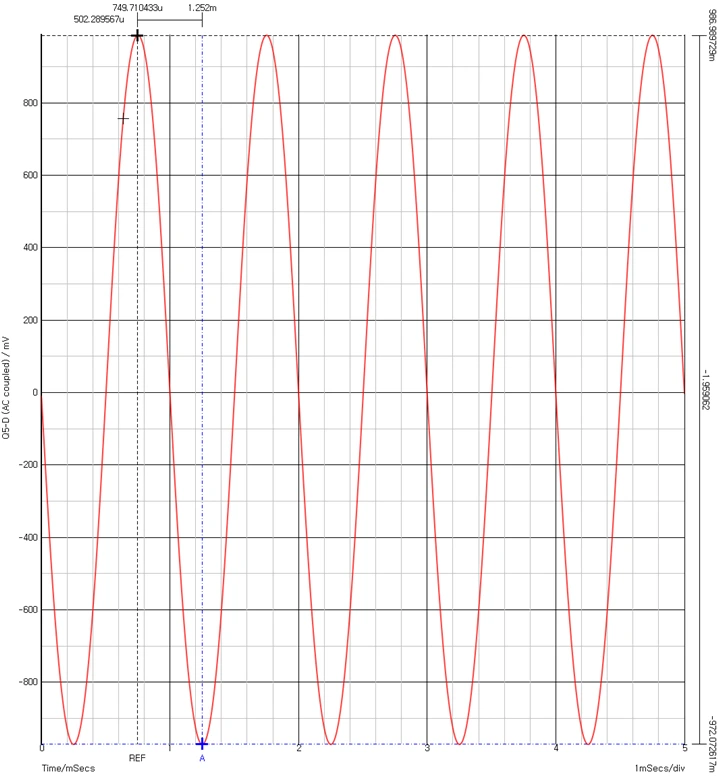
The final design achieved a gain of 65.83 dB, meeting the 60 dB-or-more requirement.

5. Discussion
I designed an amplifier with a differential input and a single-ended output under the requirement of 60 dB or more of gain. The first stage is a differential amplifier with an active load, and the second stage is a source-coupled amplifier. The result is an amplifier that produces a 1.96 Vpp output signal for a 1 mVpp input signal. Its gain is 65.83 dB, which meets the 60 dB-or-more requirement.
Above all, working through this design deepened my understanding of differential amplifiers and basic amplifier biasing, which I learned in Electronic Circuits II.