Chapter 1: CMOS Overview (Complementary Metal Oxide Semiconductor)
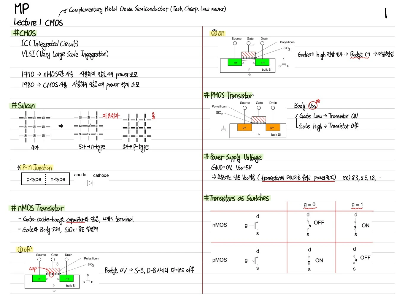
CMOS (Complementary Metal Oxide Semiconductor) is the standard technology for today's microprocessors and semiconductor circuits, with three key properties: fast, cheap, and low power. These notes cover everything from the CMOS process to nMOS/pMOS transistor operation, the switch model, and CMOS gate design.
ICs and VLSI
- IC (Integrated Circuit): many transistors, resistors, and capacitors integrated on a single silicon chip
- VLSI (Very Large Scale Integration): integrating millions of transistors or more on a single chip
How the Technology Changed
- 1970s: only nMOS was used → it consumed power even when idle (static power consumption)
- 1980s onward: CMOS adopted → almost no power consumed when idle (the biggest advantage of CMOS)
Silicon and the P-N Junction
Silicon is a group IV element. Doping a pure Si crystal with a group V element (phosphorus, arsenic, etc.) leaves free electrons and makes it n-type; doping it with a group III element (boron, etc.) leaves holes and makes it p-type.
P-N Junction
Joining p-type and n-type material forms a diode. Current flows in only one direction (anode → cathode).
nMOS Transistor
- The gate-oxide-body stack is the same as a capacitor (four terminals: G, S, D, B)
- The gate and body are conductors, and SiO₂ is a good insulator
nMOS Operation
① OFF (Gate Low):
Source, Gate, Drain — Polysilicon, SiO₂ layer- The body is at 0V → the S-B and D-B diodes are OFF → no current flows
② ON (Gate High):
- A high voltage is applied to the gate → the body surface inverts to (-) → a channel forms → current flows between S and D
pMOS Transistor
It works the opposite way from nMOS.
- The body is at V_DD
- Gate Low → transistor ON
- Gate High → transistor OFF
Power Supply Voltage
- GND = 0V, V_DD = 5V (traditional)
- → Recently, lower V_DD is used (less damage to transistors and lower power): e.g., 3.3, 2.5, 1.8V
Transistors as Switches
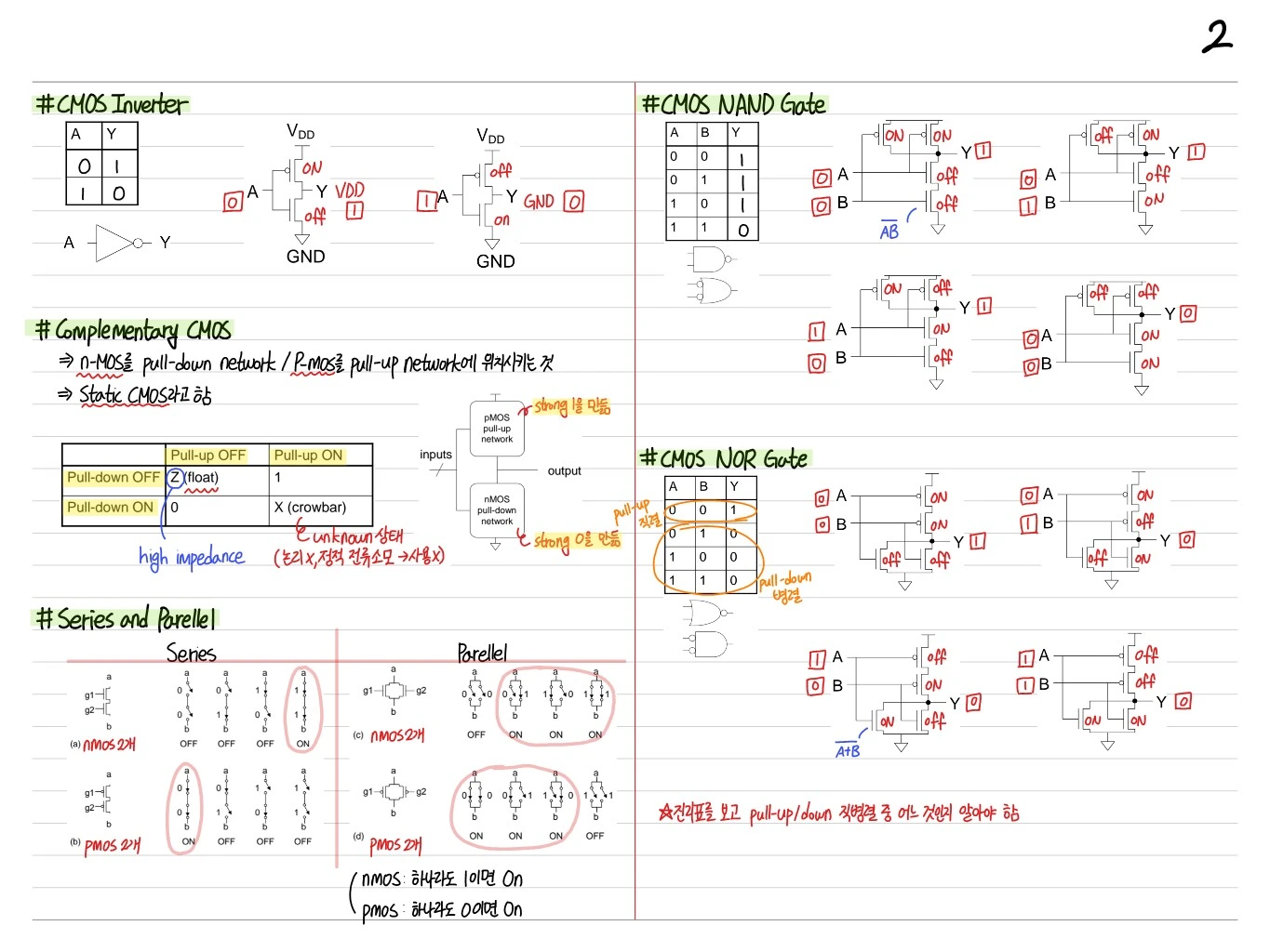
In CMOS design, transistors are abstracted as switches:
| g=0 | nMOS | pMOS |
|---|---|---|
| OFF | ON | - |
| g=1 | nMOS | pMOS |
|---|---|---|
| ON | OFF | - |
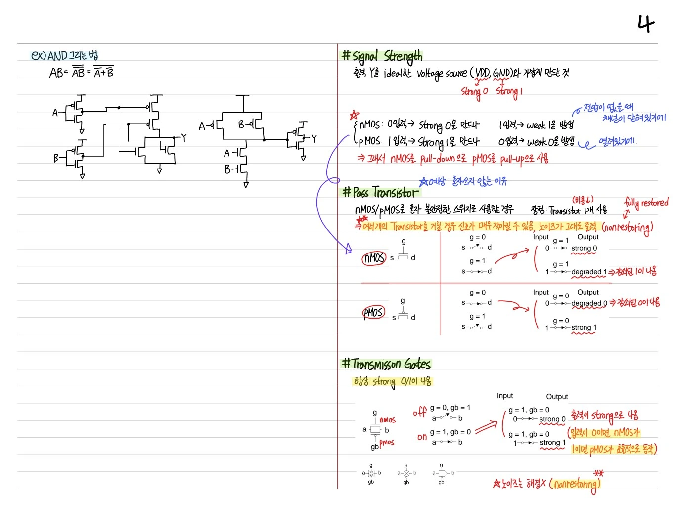
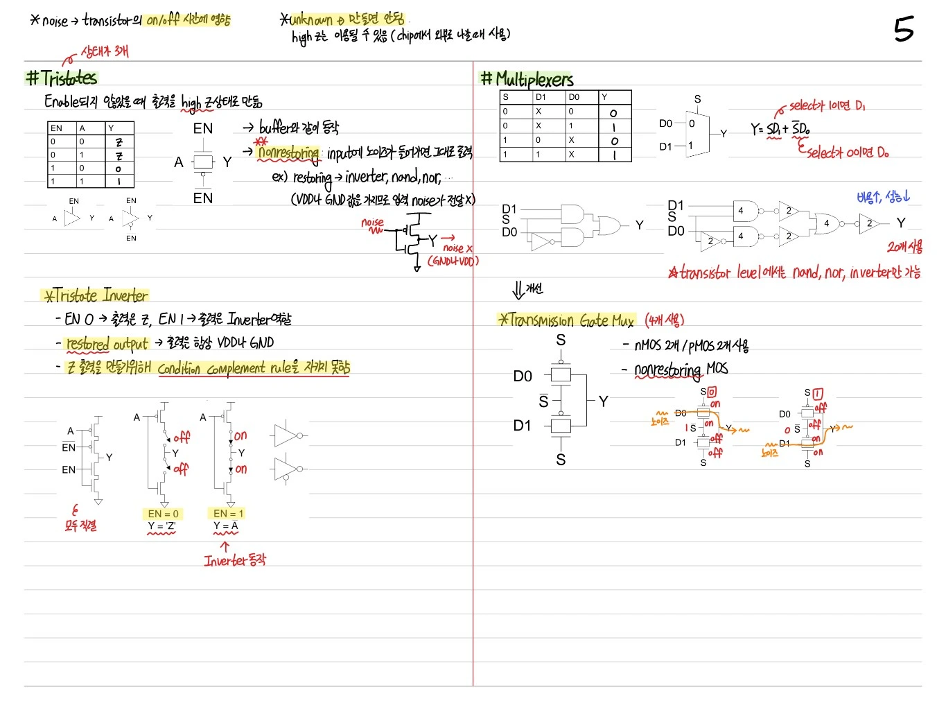
nMOS is ON when g=1 (passes 0 well), and pMOS is ON when g=0 (passes 1 well). This property is the heart of CMOS complementarity.
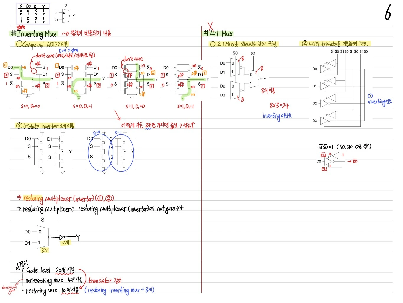
The CMOS Inverter and Basic Gates
CMOS inverter (NOT gate):
       V_DD
        │
       [pMOS]
        │
   A ───┼──── Y = NOT A
        │
       [nMOS]
        │
GND- A=0 → pMOS ON, nMOS OFF → Y=V_DD (1)
- A=1 → pMOS OFF, nMOS ON → Y=GND (0)
Why CMOS Saves Power
- In the static state (when A is not changing), only one of the pMOS and nMOS is ON → the current path is broken → static power = 0
- Short-circuit current flows only while the transistors switch
This is why CMOS uses far less power than nMOS-only logic.
Compound Gates: NAND, NOR, XOR, and More
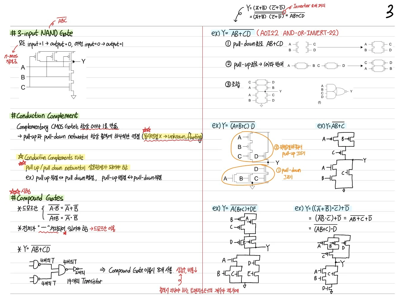
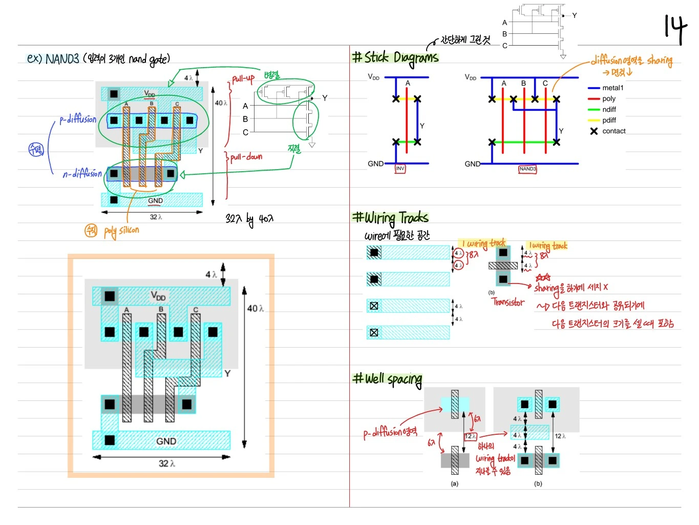
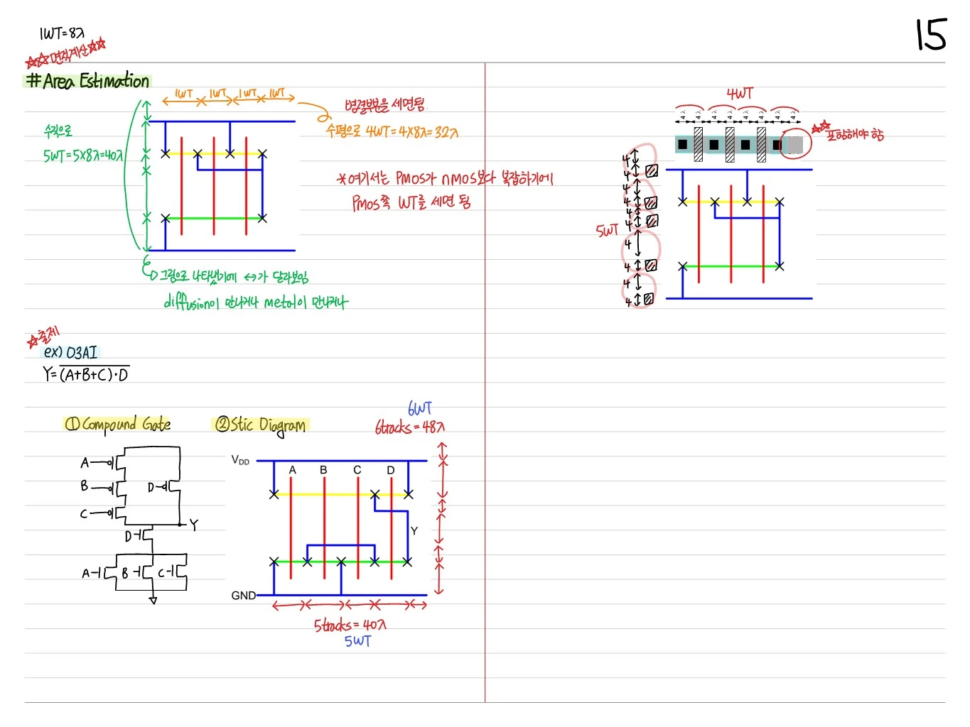
CMOS gates consist of a pull-up network (pMOS) and a pull-down network (nMOS):
- Pull-up: connects
Yto V_DD (pMOS) - Pull-down: connects
Yto GND (nMOS)
The two networks are complements of each other.
- NAND: pull-down = A·B (series), pull-up = A+B (parallel)
- NOR: pull-down = A+B (parallel), pull-up = A·B (series)
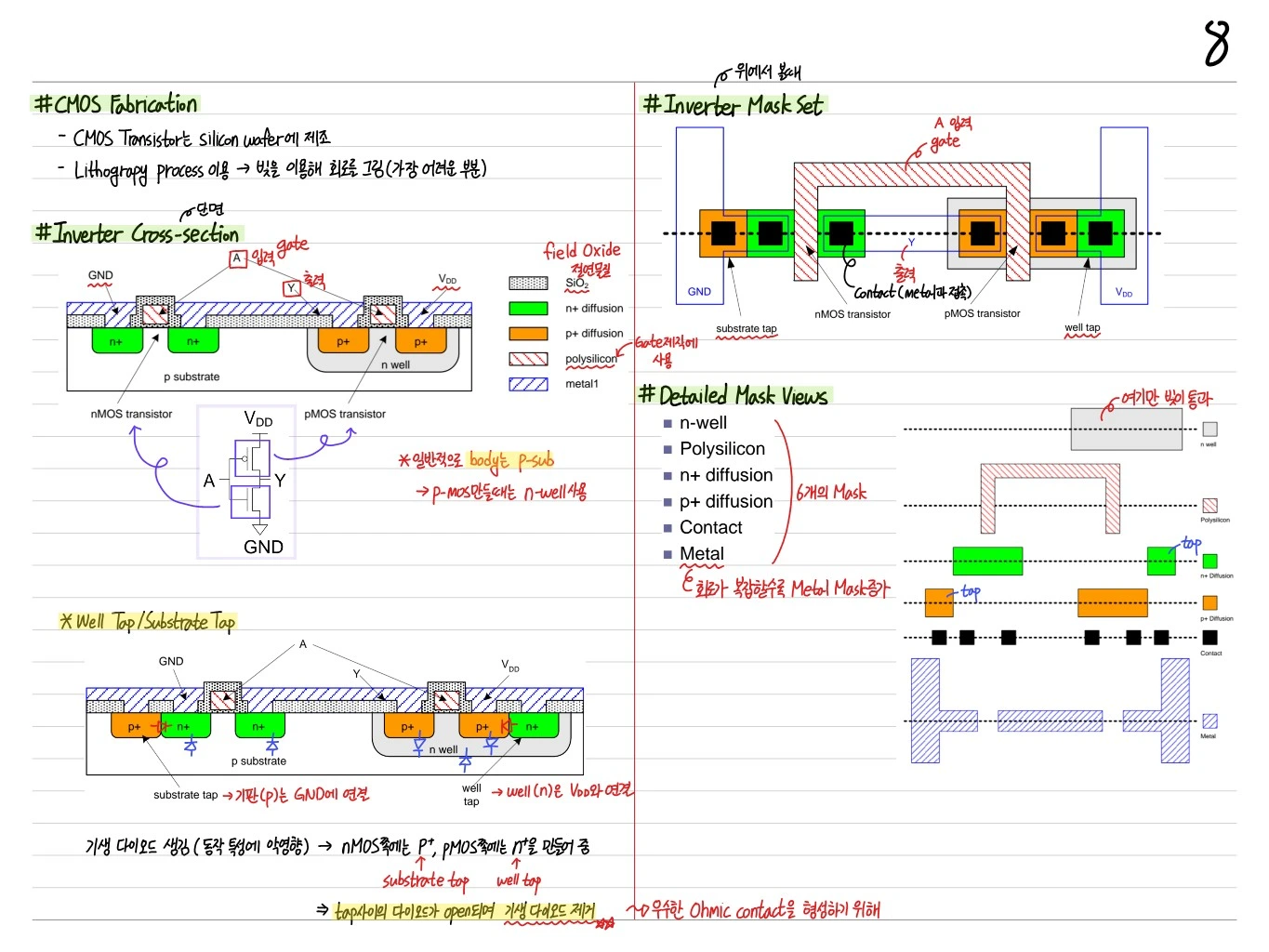
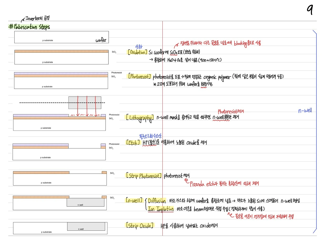
CMOS Process Cross-Section
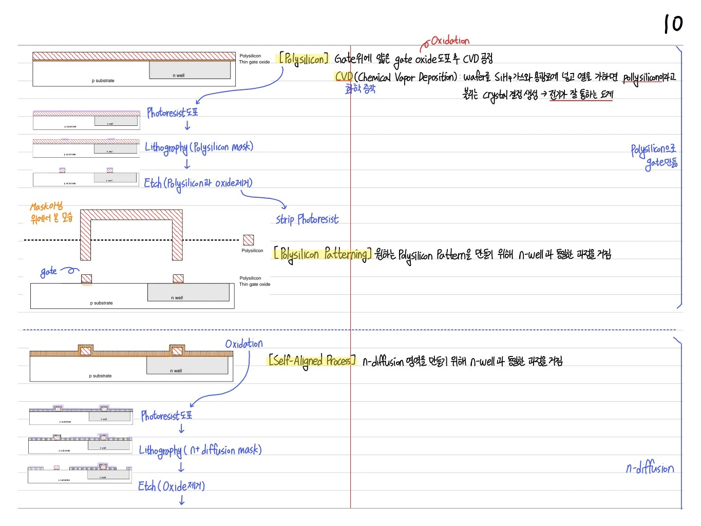
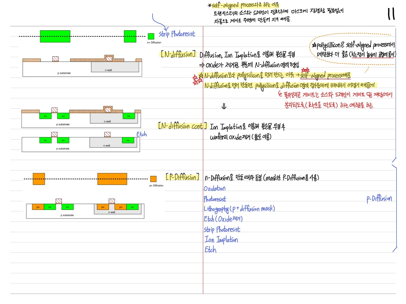
- An N-well is formed on the P-substrate, and the pMOS P+ source/drain sit inside it
- The nMOS N+ source/drain sit outside, in the substrate
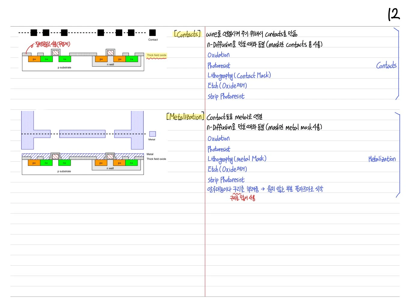
- Each region is connected through the polysilicon gate, SiO₂ insulator, and metal interconnect
Noise Margin and the Voltage Transfer Characteristic (VTC)
The voltage transfer characteristic of CMOS logic:
- V_OL: output low level
- V_OH: output high level
- V_IL: input low threshold
- V_IH: input high threshold
- Noise Margin high = V_OH - V_IH
- Noise Margin low = V_IL - V_OL
CMOS swings rail to rail (0~V_DD), so its noise margins are very good.
Propagation Delay
- t_pHL: time until the output switches from H to L
- t_pLH: time until the output switches from L to H
- t_p = (t_pHL + t_pLH) / 2
The delay is set by the load capacitance C_L and the charging current I:
Power Dissipation
CMOS power consumption:
- Switching (dynamic):
- Short-circuit: the moments during switching when PMOS and NMOS are ON at the same time
- Leakage (static): grows as the process shrinks (important)
Reducing Power
- Lower V_DD (most effective, since it is squared)
- Lower clock frequency
- Lower capacitance (layout optimization)
- Control leakage (threshold voltage tuning)
Sizing
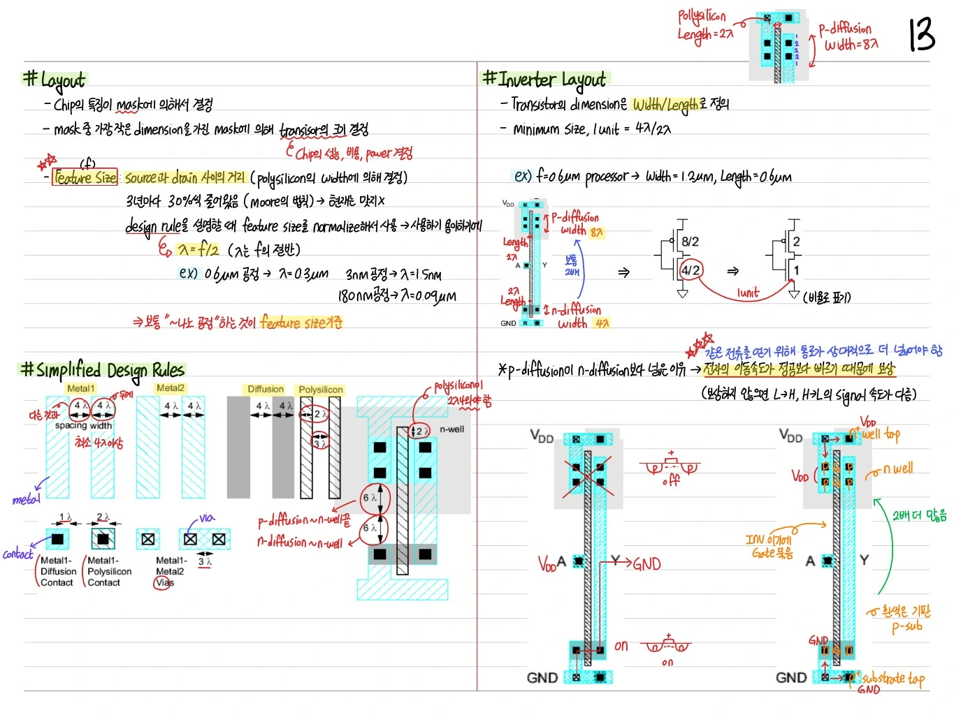
A transistor's W/L ratio sets its driving strength:
- Larger W (channel width) → more current → faster
- Larger L (channel length) → less current → slower, lower leakage
Balancing pMOS / nMOS
- pMOS hole mobility < nMOS electron mobility (by about 2~3x)
- For the same driving strength, make the pMOS W 2~3x larger
Layout Design
- Multiple routing layers such as Metal1 and Metal2
- Contacts and vias connect the layers
- Follow the design rules (minimum spacing, overlap, etc.)
Interconnect Delay
In advanced processes, wire delay exceeds gate delay. The RC delay model:
- Wire length ↑ → delay ↑ quadratically
- Optimized with buffer insertion and wire sizing
Clock Distribution
The clock must reach every flip-flop at the same time. Skew is minimized with an H-tree, a clock grid, and similar structures.
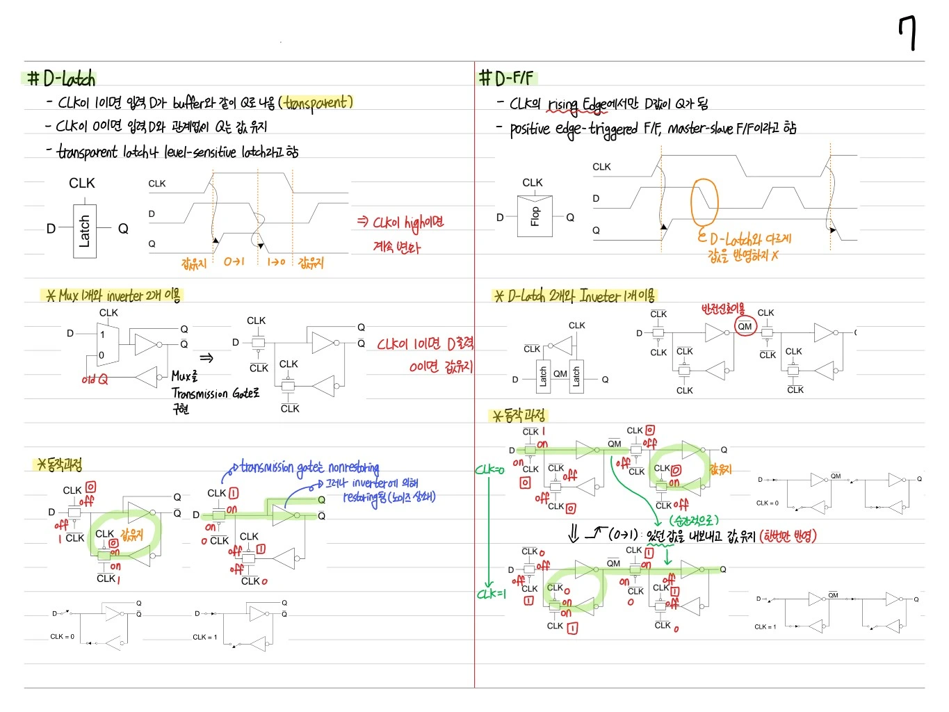
Latches and Flip-Flops
- Latch: level-triggered. Transparent while the clock is at its active level
- Flip-Flop: edge-triggered. Captures data only on the rising/falling clock edge
A standard CMOS flip-flop is built from two latches in a master-slave arrangement.
Setup Time, Hold Time
- Setup time (t_su): the minimum time D must be stable before the clock edge
- Hold time (t_h): the minimum time D must be held after the clock edge
Timing analysis:
- Max path: t_cq + t_comb + t_su < T_clk → setup constraint
- Min path: t_cq + t_comb > t_h → hold constraint
Scaling
Moore's law: the transistor count doubles every two years. To get there, the feature size (L) shrinks by 0.7x each generation using constant-field scaling or constant-voltage scaling.
- Faster transistors
- Lower power per transistor
- But more leakage and more wire delay → new design techniques are needed (FinFET, etc.)
The Future of CMOS
- FinFET / GAAFET (Gate-All-Around): 3D structures that control leakage in advanced processes
- Low-power design techniques: clock gating, power gating, DVFS (Dynamic Voltage Frequency Scaling)
- Multi-V_T: use different V_T values depending on the speed vs. power trade-off
Summary
| Concept | Key point |
|---|---|
| CMOS = Complementary MOS | Complementary nMOS + pMOS structure |
| nMOS: ON at g=1, passes 0 well | pMOS: ON at g=0, passes 1 well |
| Static power ≈ 0 | No current path in the static state |
| Dynamic power: | Lowering V_DD is most effective |
| Sizing | W/L sets driving strength, pMOS W 2~3x |
| Timing: Setup/Hold, Clock skew | The most important constraint in every process |
CMOS is the physical foundation of microprocessor design, and all digital logic, RTL design, and computer architecture that follow are built on top of it.