1. Topic
Choice of topic Designing an AI hardware accelerator that performs AI computation quickly
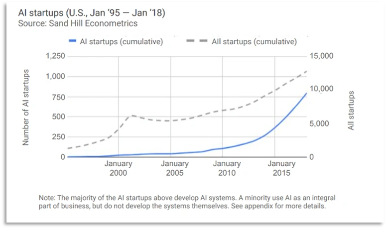
An AI accelerator speeds up the computation in artificial intelligence (AI) algorithms. AI processes huge amounts of data and performs complex tasks, so it needs enormous compute power. General-purpose CPUs or GPUs alone struggle to handle this computation efficiently.
That is why AI accelerators are needed. An AI accelerator is hardware specialized for AI workloads, enabling higher performance and lower energy consumption. It greatly shortens the training and inference time of AI algorithms and improves the performance of AI applications. AI accelerators are therefore essential to the advancement and adoption of AI.
2. Design Flow
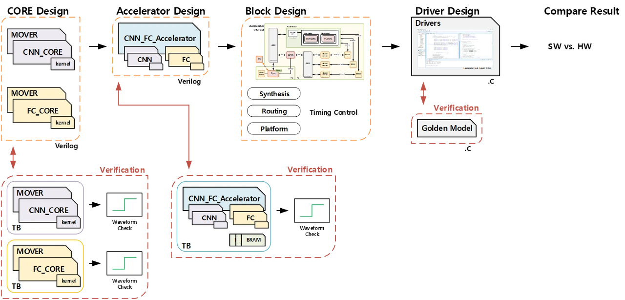
I designed a CORE containing kernels that can perform CNN and FC operations, then designed a MOVER to move data to and from it. Along the way, each CORE and MOVER was verified.
The CNN and FC COREs and their MOVERs were then combined into a single Accelerator. AXI-lite was used for hardware control, and the accelerator is controlled through a memory map.
Using the resulting Accelerator IP, I built the system in a block design.
After that, I wrote a SW driver so the hardware could actually be operated.
(I verified that the design was correct by comparing the hardware's results against a golden model.)
3. HW System
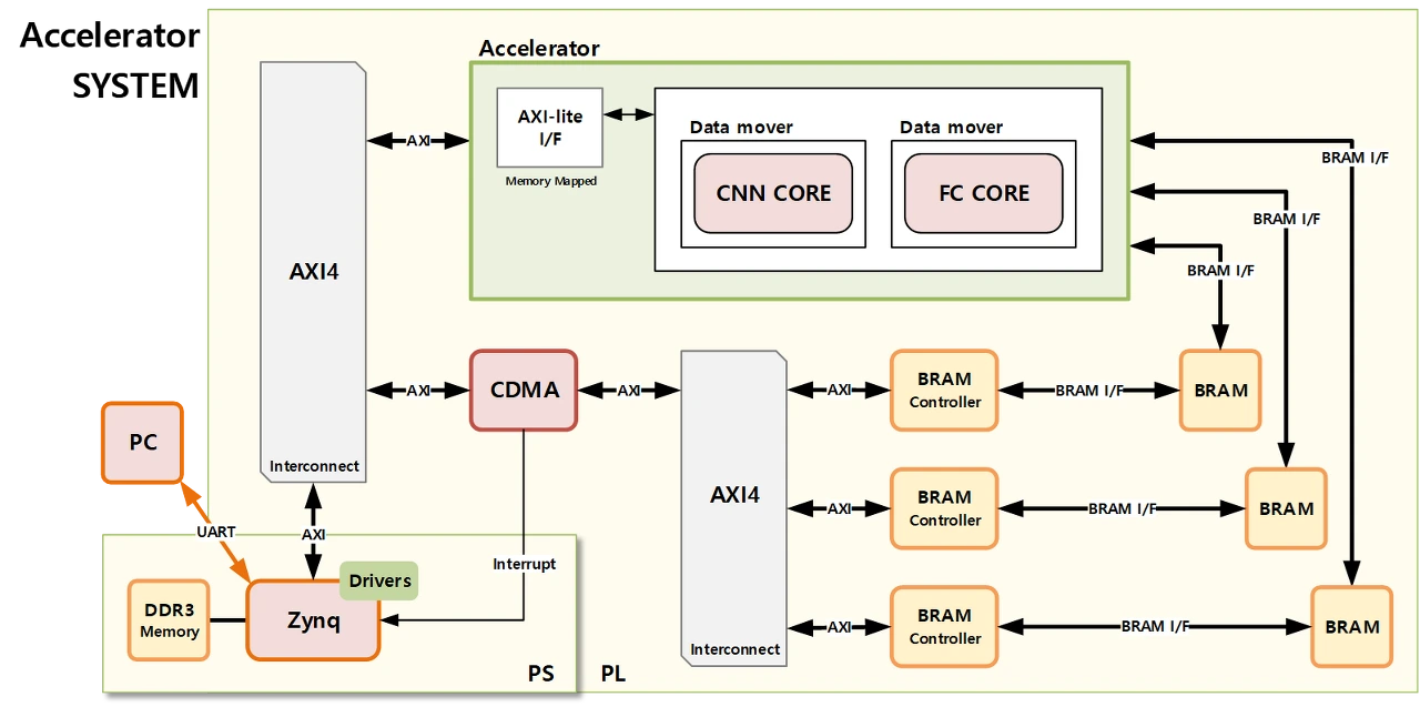
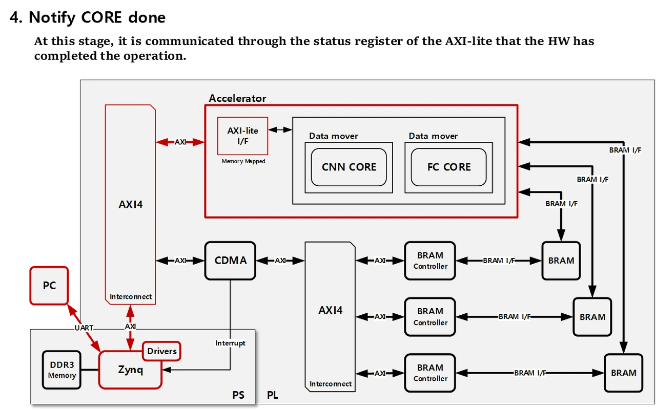
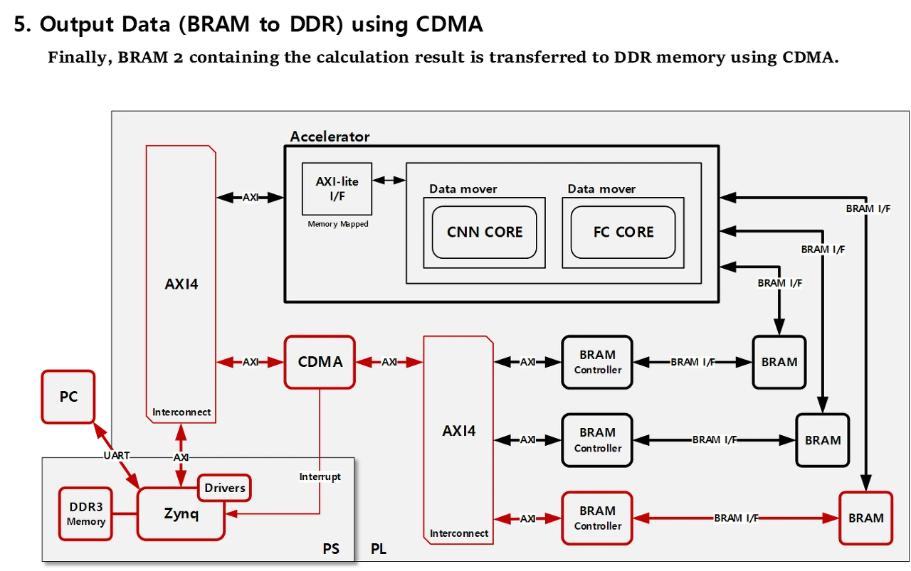
Zynq : an FPGA chip made by Xilinx that offers a PS and a PL region. The PS region is the processor side, where a Cortex processor is available. The PL region is where user-described hardware is implemented.
AXI4 : the protocol that handles communication between IPs.
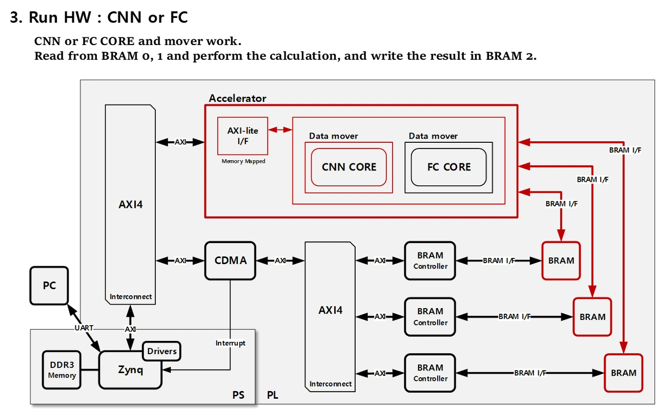
BRAM : a buffer that stores the data needed for computation.
BRAM Controller : an IP that provides an interface for reading and writing BRAM.
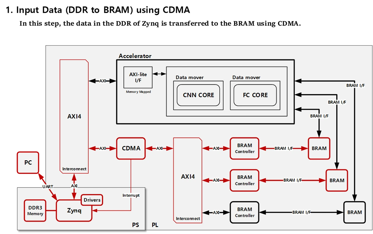
CDMA : used to move data from DDR memory to BRAM. Once given a command, the CDMA moves data independently of the system processor, using the AXI protocol. When the CDMA finishes a transfer, it signals completion with an interrupt.
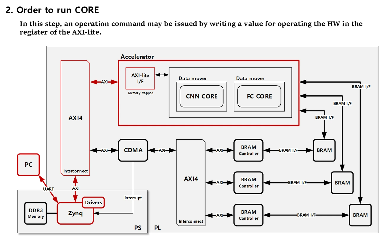
Accelerator : the IP of the accelerator I designed, controlled through AXI-lite.
4. HW Processing
This is how the designed system operates.
5. Accelerator Scheme
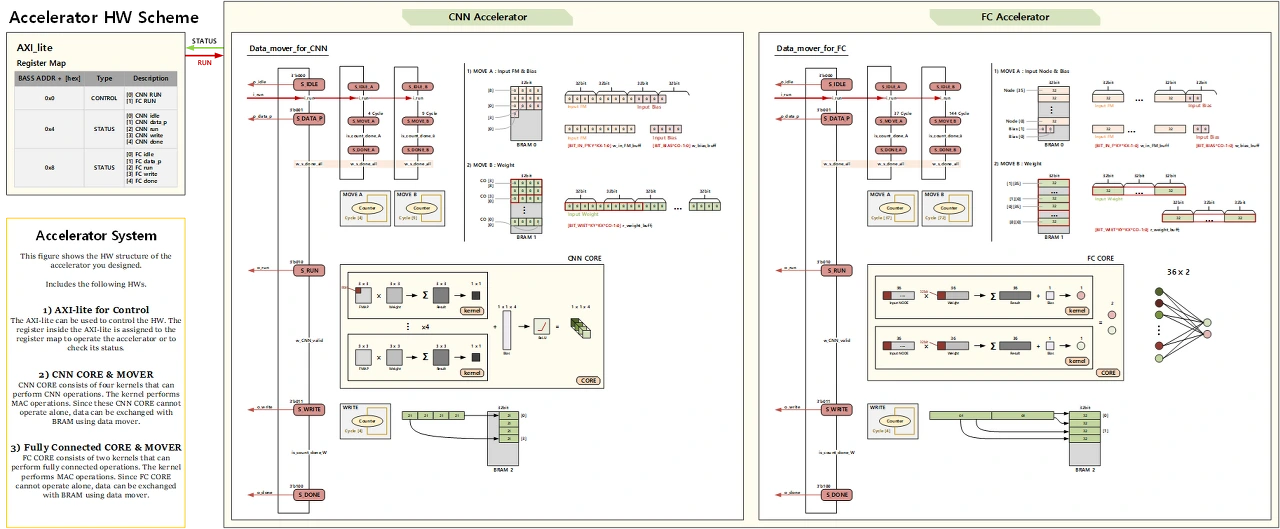
A detailed look at the structure of the Accelerator IP.
1) Memory Map
The accelerator is controlled by writing and reading registers inside its AXI-lite interface.
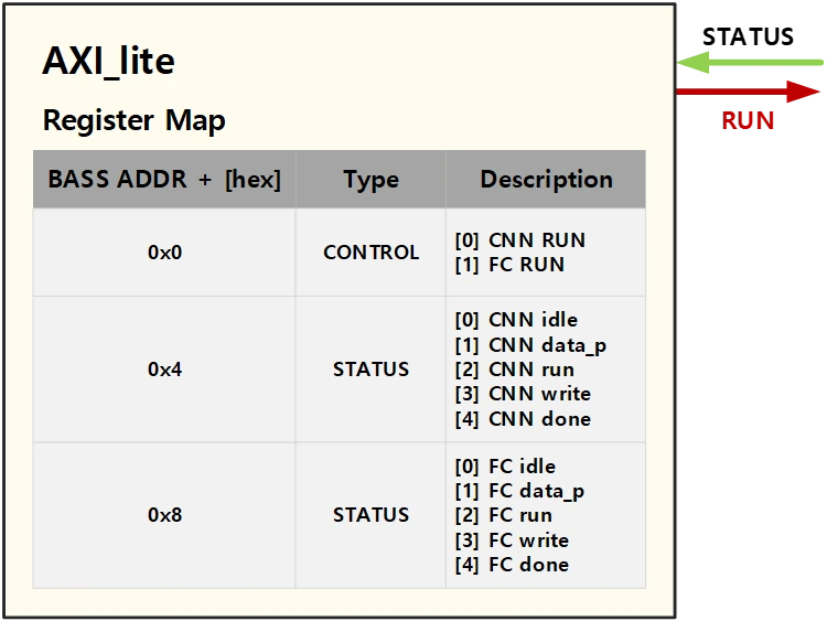
0X0: the control register, which issues run commands to the CNN/FC COREs.0X4: a status register for checking the CNN CORE's operation.0X8: a status register for checking the FC CORE's operation.
2) CNN Core/Data Mover
# CNN CORE
In typical CNN computation, the input feature map is larger than 3x3. The figure below shows such a structure.
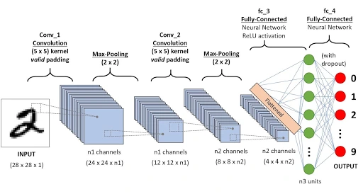
Taking the model above as an example, the input feature map is 28x28. Accelerators that can run such a large model in one go do exist and can be designed, but they need a great deal of FPGA resources. So the usual approach is to design an accelerator called a CNN CORE and reuse this CORE many times to improve resource efficiency.
The CORE is built in hardware and performs its computation in the FPGA's PL region. An example of such a CORE structure is shown below.
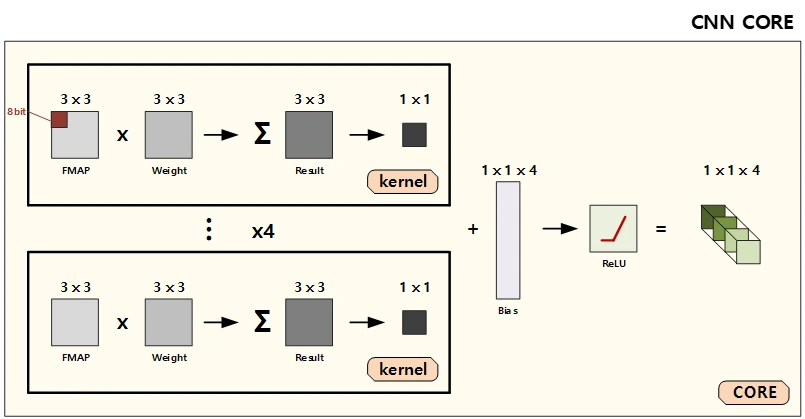
This is the CORE we designed, and its structure can be changed depending on the goals. The CORE designed here performs 3x3 operations, built in hardware in the FPGA's PL region. Does that mean it cannot handle input feature maps larger than 3x3? No. If a 5x5 input feature map is needed, the software side can slice it up and feed it to the 3x3 CORE 9 times.
As for the structure of the CORE: first, the 3x3 input feature map and the 3x3 weights are multiplied element by element. This produces a 3x3 result, which is then accumulated. That is the kernel's job: multiply and accumulate. These kernels are computed in parallel, as many as the CORE has outputs. In the example in the figure, the multiply-accumulate is performed 32 times in parallel. After this parallel computation, the bias is added and the result passes through the activation function, which completes the CORE's operation. (No activation function was used in the CORE designed here.)
(Note) Code is not provided in this post. __
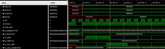
Test Bench
# CNN Data Mover
The CNN CORE cannot be used on its own, because it has no interface for reading and writing data from BRAM. A DATA MOVER with an interface for reading and writing data from BRAM is therefore needed. The module that connects and contains this DATA MOVER and the CORE is the CNN CORE MOVER designed here. The structure of the CNN CORE MOVER is shown below.
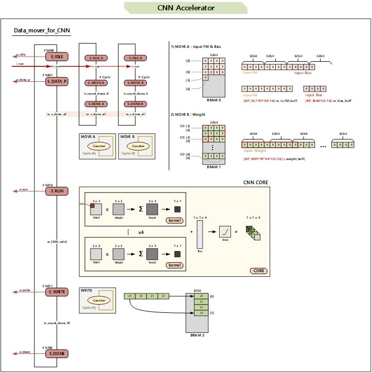
The hardware starts when the RUN signal arrives.
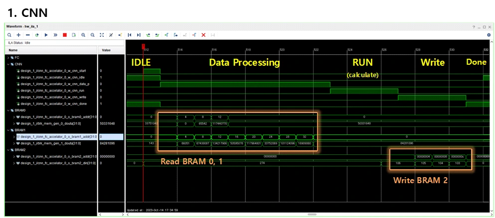
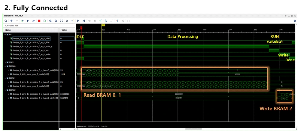
The MOVER has five states: IDLE, DATA_Processing, RUN, WRITE, and DONE. To implement it in hardware, I designed an FSM that transitions between these states. Each state does the following:
IDLE : waiting
DATA_Processing : fetches data from BRAM into a buffer so it can be fed to the CORE all at once
RUN : the CORE is running (performing the CNN computation)
WRITE : writes the CORE's results back to BRAM
DONE : signals that all operations are complete
Test Bench
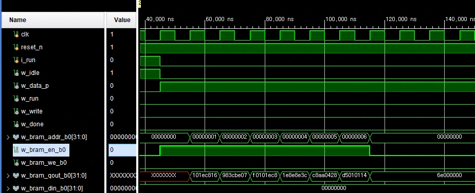
Output signals of BRAM0, showing the values written to each address.
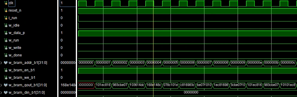
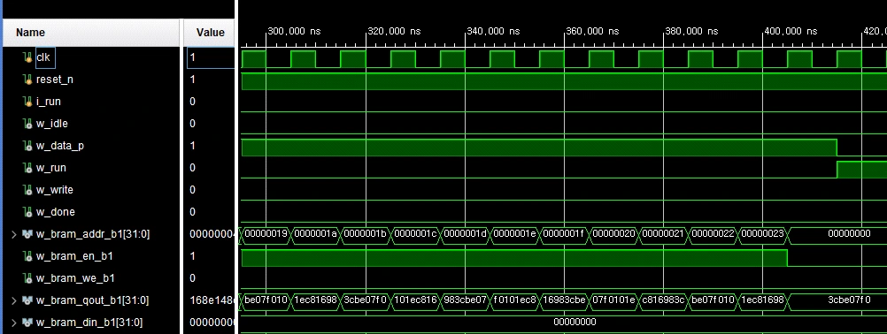
Output signals of BRAM1, showing the values written to each address.
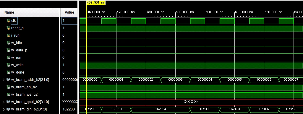
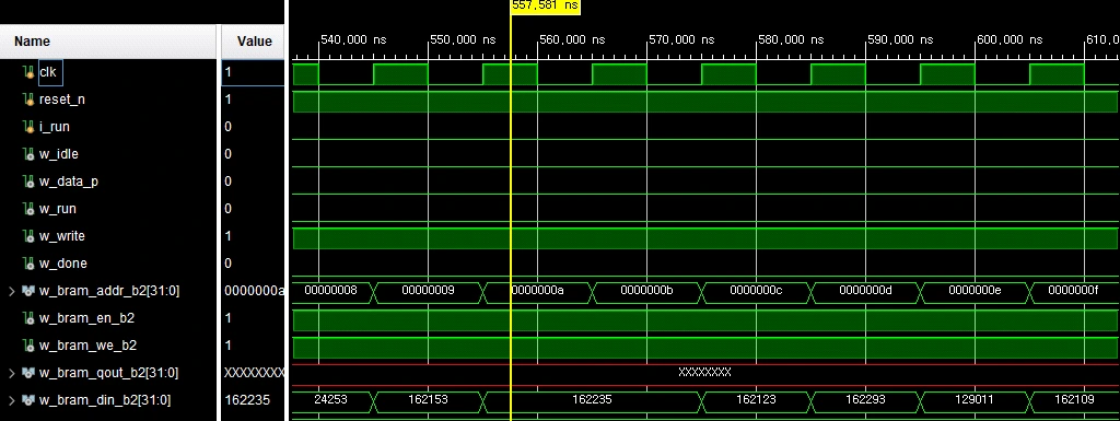
Output signals of BRAM2, showing the values written to each address.
3) FC Core/Data Mover
# FC CORE
The FC (fully connected) operation is commonly used in the final stage of an AI model. Where CNN is a 2D MAC operation, FC is a 1D MAC operation. The figure below shows the structure of the FC CORE.
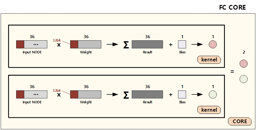
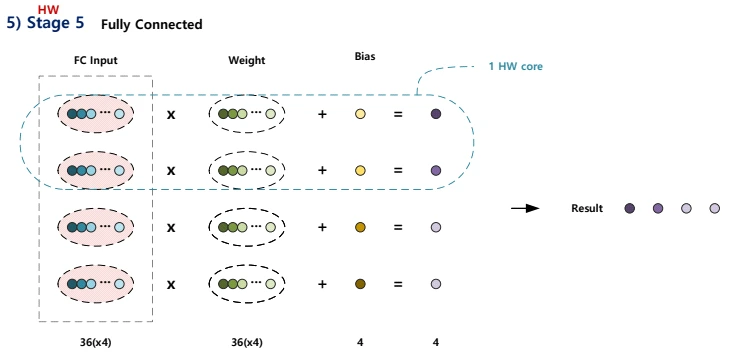
Like the CNN CORE, the FC CORE consists of inputs, weights, and a bias. The FC structure I designed has two kernels, each of which accumulates 36 input-weight products and adds a bias. With two kernels, one CORE operation produces two results.
# FC Data Mover
The FC CORE designed above performs 1D MAC operations. But the FC CORE cannot be used on its own either, because it has no interface for reading and writing data from BRAM. A DATA MOVER with an interface for reading and writing data from BRAM is therefore needed. The module that connects and contains this DATA MOVER and the CORE is the FC CORE MOVER designed here. The structure of the FC CORE MOVER is shown below.
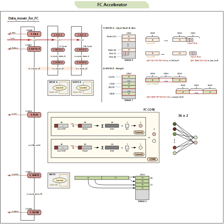
Test Bench
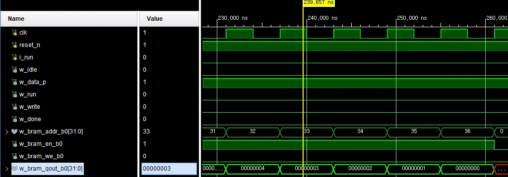
Output signals of BRAM0, showing the values written to each address.
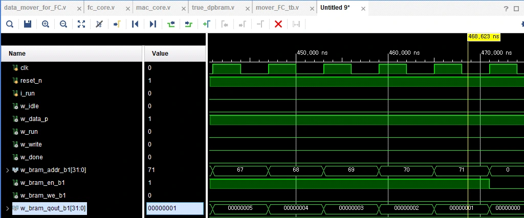
Output signals of BRAM1, showing the values written to each address.
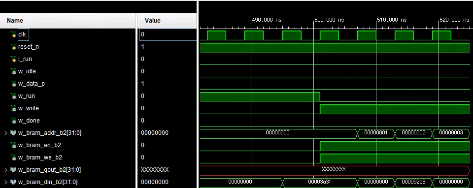
Output signals of BRAM2, showing the computed results written to each address.
5. AI Model Design
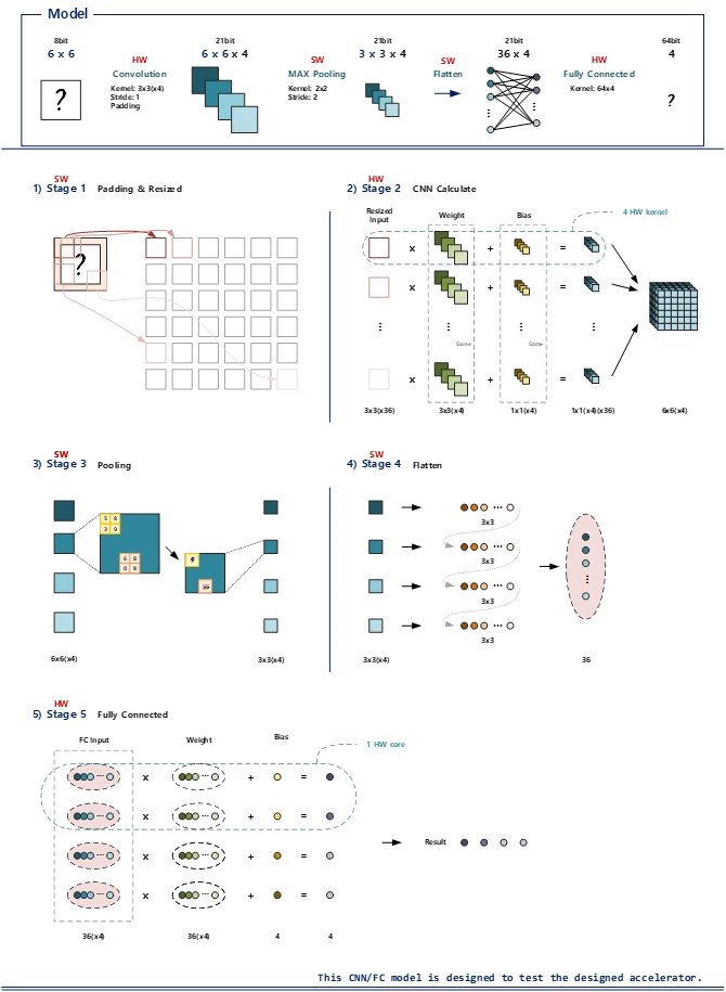
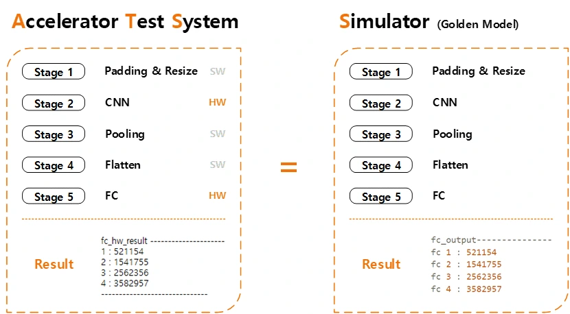
In this model, only the CNN and FC operations run in hardware; everything else is handled in software. Each operation is performed as follows.
1) Stage 1
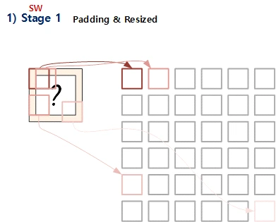
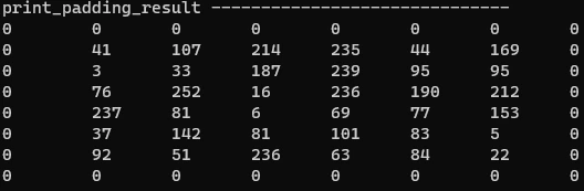
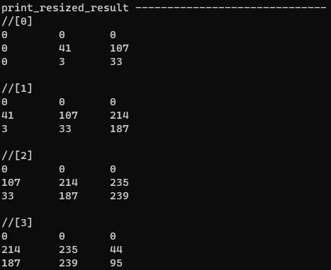
Stage 1 pads the given 6x6 input and rearranges it into six 3x3 tiles.
This is a preprocessing step that slices the input so it can be fed to the hardware.
2) Stage 2
Stage 2 runs the CNN operation in hardware on the resized result from Stage 1.
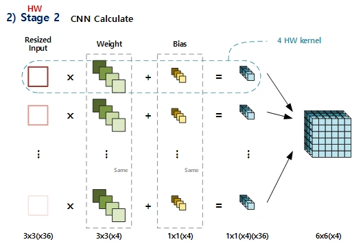
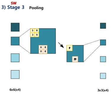
3) Stage 3
Stage 3 applies a pooling operation in software to the result of Stage 2.
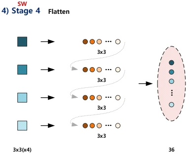
4) Stage 4
Stage 4 applies a flatten operation in software to the result of Stage 3.
5) Stage 5
Stage 5 runs the fully connected operation in hardware on the result of Stage 3.
6. C Simulator Design
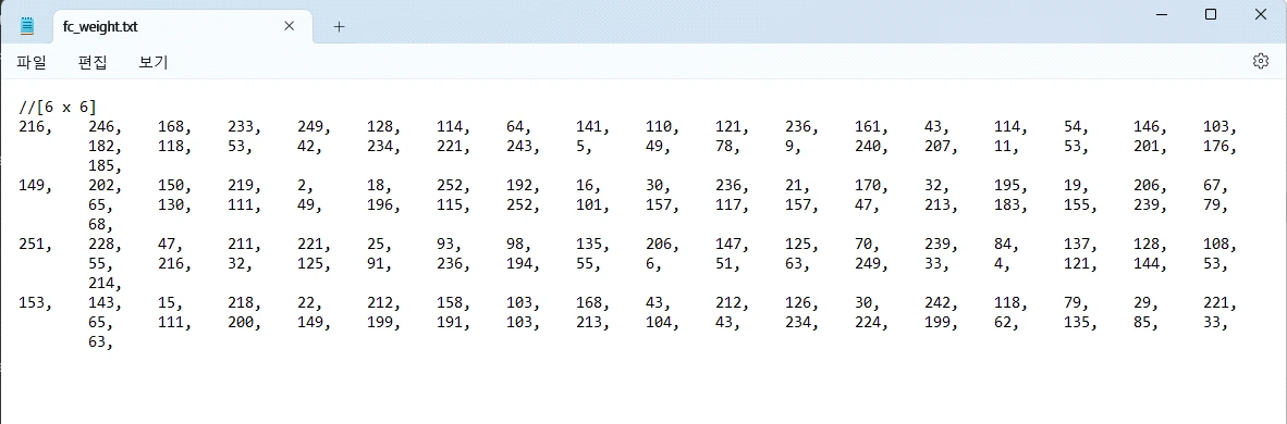
The simulator written in C verifies that the hardware was designed correctly.

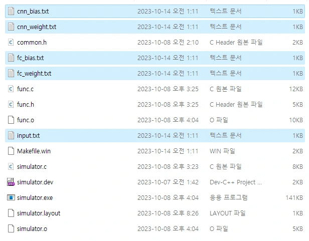
It generated the data below, which can be used for verification.
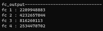
The code's computed results can be checked in the terminal. Here they are.
7. C Driver and Main System Design
I wrote a driver to control the hardware and implemented the AI model in C.
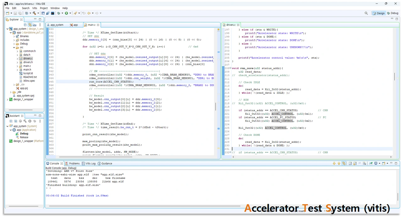
The key code is as follows.
cdma_controller((u32 *)ddr.flatten_output, (u32 *)CDMA_BRAM_MEMORY0, "DDR0 to BRAM0", 4*FC_BRAM0_CYCLE);
Code that moves data between BRAM and DDR with the CDMA
if (status_addr == ACCEL_CNN_STATUS) // CNN
	Xil_Out32((u32) ACCEL_CONTROL, (u32)0x1);
if (status_addr == ACCEL_FC_STATUS) // FC
	Xil_Out32((u32) ACCEL_CONTROL, (u32)0x2);
Xil_Out32((u32) ACCEL_CONTROL, (u32)0x0);
Code that starts the selected core
8. Verification
1) Waveform
By including Vivado ILA in the system, I could trigger on signals for debugging. The waveforms are shown below.
2) Golden Model Comparison
I wrote a golden model in C and verified the system by comparing its results with the system's output.
9. Result
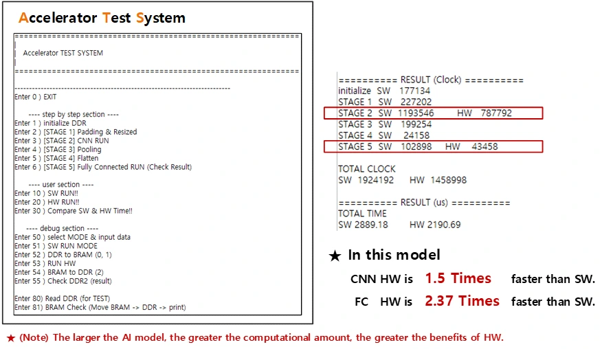
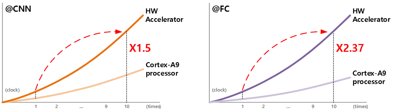
I designed an accelerator that performs AI computation quickly, and verification confirmed that it was designed correctly. There were many bugs along the way, and they took a lot of time. Comparing the final hardware against software, the accelerator was 1.5x faster than software for the CNN operation and 2.37x faster for the FC operation. This shows the benefit of an accelerator: it computes faster than software.
10. Conclusion
The AI accelerator did not reach the performance gap over software that I had hoped for, due to various constraints and limitations, but there are ways to address them. I also expect the advantages of AI accelerators to stand out more as data volumes and compute requirements grow. Better results should be possible especially with research and investment at the company level rather than by an individual.
AI accelerators are recognized as an important tool for processing large volumes of data effectively. They can efficiently handle data at a scale that CPUs alone struggle with, and are expected to play a central role in AI. GPUs, meanwhile, consume a lot of power and are mostly specialized for simple operations, which limits them for AI workloads that involve large, complex models or many different kinds of operations. These constraints are increasingly emphasized in the AI field and drive the need for new AI accelerators. Accelerators built on FPGAs or ASICs can implement hardware optimized for specific operations, achieving better speed and power efficiency than GPUs.
Because of these characteristics, new kinds of AI accelerators are increasingly seen as essential in the era of the Fourth Industrial Revolution. Continued development and research on accelerators is therefore expected. AI accelerators will drive the advancement of modern technology by delivering high performance and efficiency across many applications.
Sun Hong