1. Kogge-Stone Adder
A fast adder can be achieved by implementing the adder with the fewest logic levels in its group PG network. Among tree adders, the one with the fewest logic levels is the Kogge-Stone adder, which has 4 logic levels as shown below.
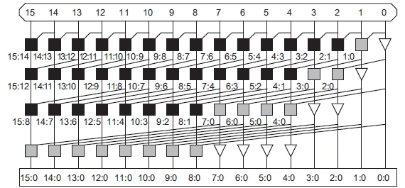
Figure 1 16-bit Kogge-Stone Adder (no Carry_in)
Source: CMOS VLSI Design: A Circuits and Systems Perspective, 4th Edition
This Kogge-Stone adder needs 8 wiring tracks, or 9 if Carry_in is included. It trades off this wiring-track cost for fast performance with few logic levels.
Below is a Kogge-Stone adder that includes Carry_in.
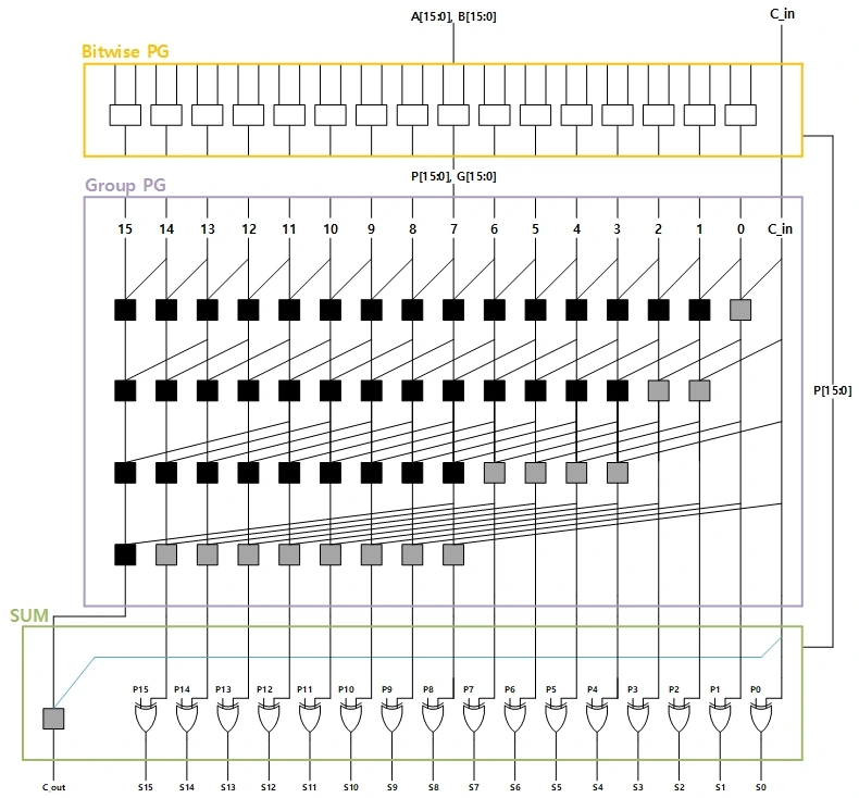
Figure 2 16-bit Kogge-Stone Adder (Carry_in)
The logic levels of the Kogge-Stone adder in Figure 2 can be reduced with higher-valency cells.
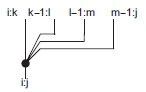
Figure 3 4-bit Higher Valency cell
2. Kogge-Stone Adder using Higher Valency Cell
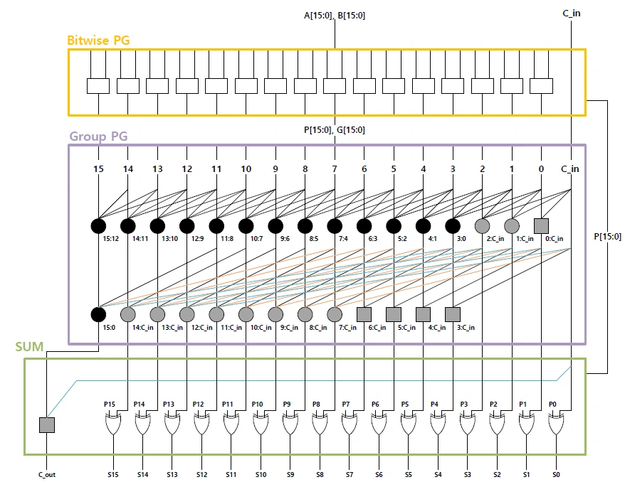
Figure 4 below shows the Kogge-Stone adder designed with higher-valency cells.
Figure 4 16-bit Kogge-Stone Adder using Higher Valency Cell
The Bitwise PG Logic performs a bitwise operation on each input to produce Propagate and Generate. These Propagate and Generate results go into the Group PG Logic, pass through the higer valency cells, and each outputs the Generate result from n down to C_in.
The black higher-valency cells in stage 2 take at most 4 inputs, so they can only output results down to 15:0. This was handled later in the SUM logic by combining G(15:0) and C_in in a gray cell to produce C_out.
Finally, the SUM logic computes the result by XORing the propagate output of the Bitwise PG Logic with the group generate output of the group PG logic.
With this design, the 4 logic levels of a regular Kogge-Stone adder were reduced to 2 logic levels.
3. Verilog Code Review
Basic Gate/Cell Define
1) XOR GATE
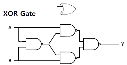
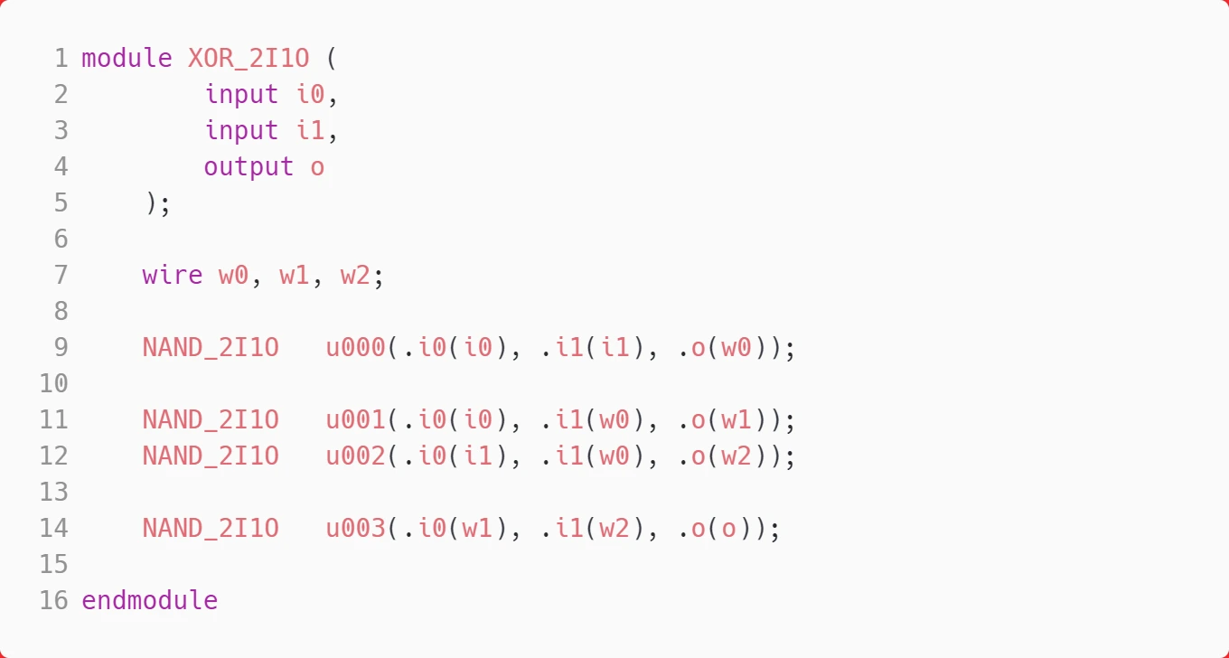
Figure 5 XOR GATE
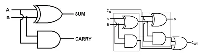
I built the XOR used in the SUM logic. Only NAND and NOR were allowed, so I designed it with NANDs as shown above.
2) Generate & Propagate Cell
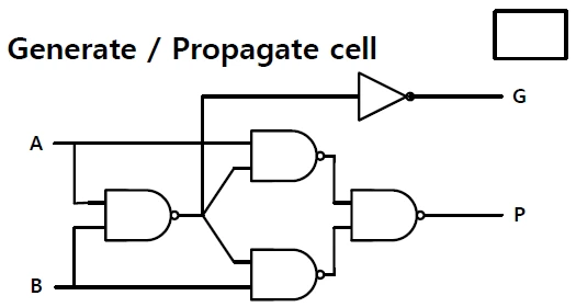
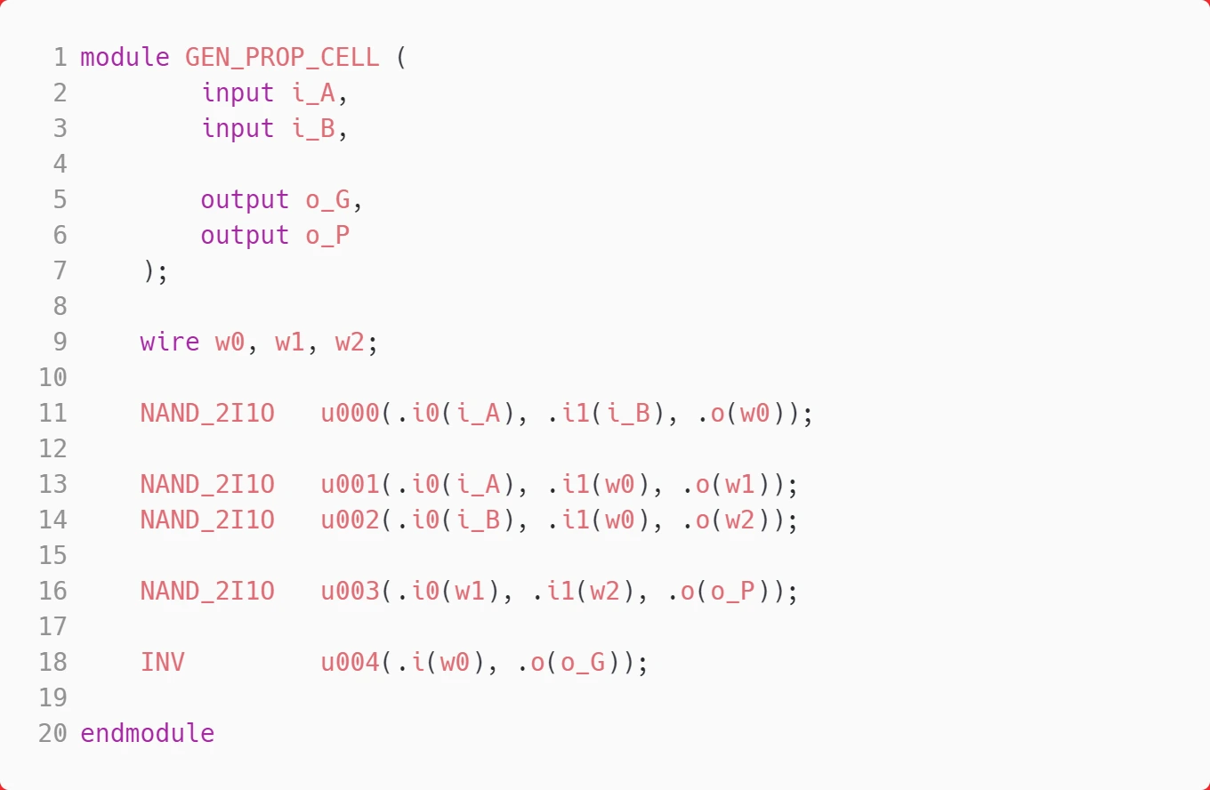
Figure 6 Generate & Propagate Cell
I defined a Generate & Propagate cell that produces the generate and propagate signals for each bit in the bitwise logic. Generate comes from an AND operation, and propagate comes from an XOR operation. I implemented it as shown above.
3) Gray Cell
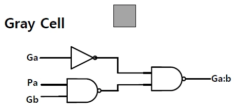
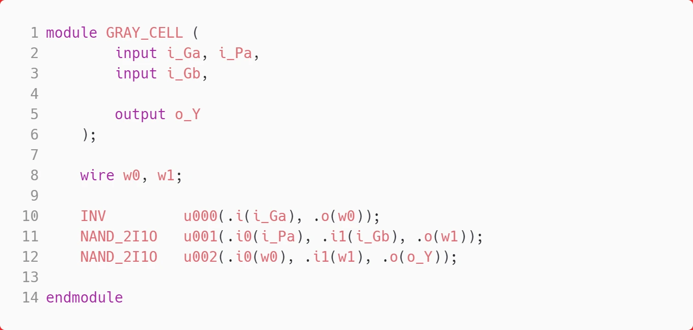
Figure 7 Gray Cell
I defined a 2-bit gray cell. It performs an AND-OR operation, which I implemented with NANDs. It computes the following logic.
Ga:b = Pa Gb + Ga
4) 3-higher valency Gray Cell
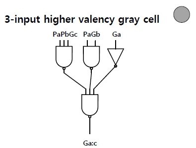
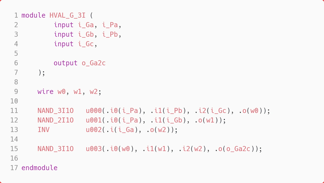
Figure 8 3-higher valency Gray Cell
I built a 3-input higher-valency gray cell that takes P and G of a, P and G of b, and G of c, and produces Generate. It computes the following logic.
Ga:c = Pa Pb Gc + Pa Gb + Ga
5) 3-higher valency Black Cell
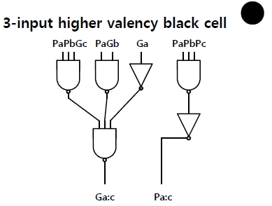
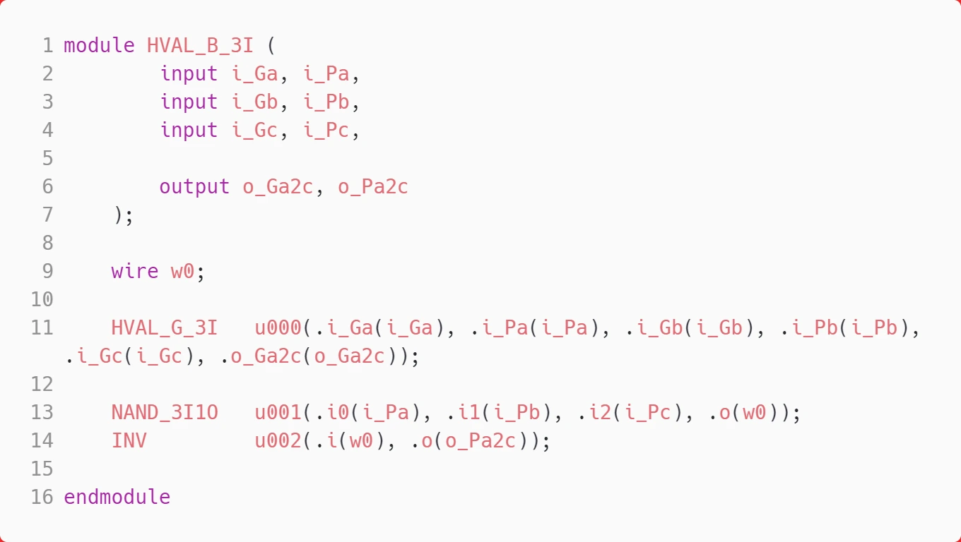
Figure 9 3-higher valency Black Cell
I built a 3-input higher-valency black cell that takes P and G of a, P and G of b, and P and G of c, and produces Generate and Propagate. It computes the following logic.
Ga:c = Pa Pb Gc + Pa Gb + Ga
Pa:c = Pa Pb Pc
It was not used in this design, but I built it for consistency.
6) 4-higher valency Gray Cell
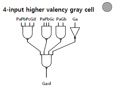
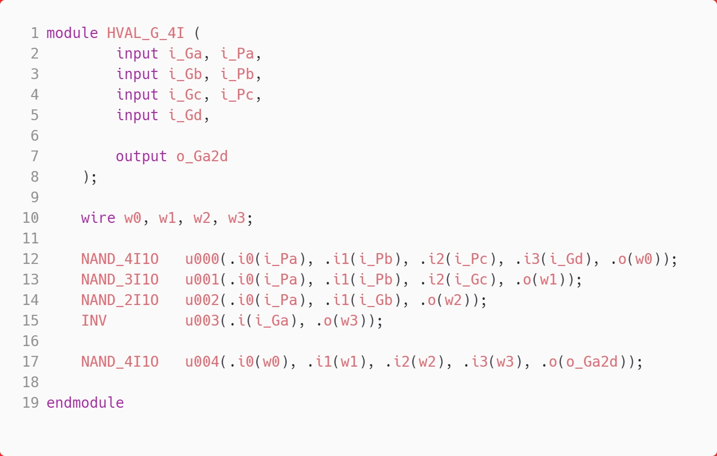
Figure 10 4-higher valency Gray Cell
I built a 4-input higher-valency gray cell that takes P and G of a, P and G of b, P and G of c, and G of d, and produces Generate. It computes the following logic.
Ga:d = Pa Pb Pc Gd + Pa Pb Gc + Pa Gb + Ga
7) 4-higher valency Black Cell
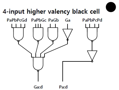
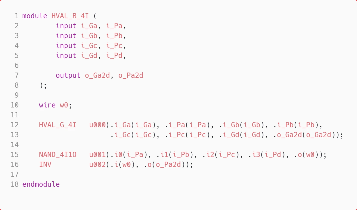
Figure 11 4-higher valency Black Cell
I built a 4-input higher-valency black cell that takes P and G of a, P and G of b, P and G of c, and P and G of d, and produces Generate and Propagate. It computes the following logic.
Ga:d = Pa Pb Pc Gd + Pa Pb Gc + Pa Gb + Ga
Pa:d = Pa Pb Pc Pd
Bitwise PG Logic
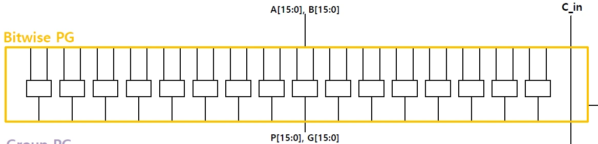
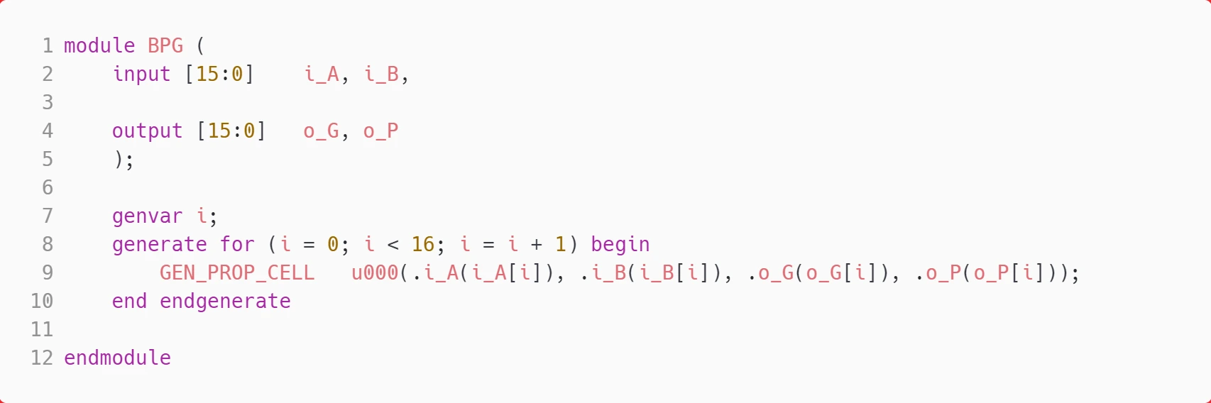
Figure 12 Bitwise PG Logic
This is the bitwise PG logic, which produces generate and propagate for each input bit. The logic for each of bits 0 to 15 was implemented with a generate statement.
Group PG Logic
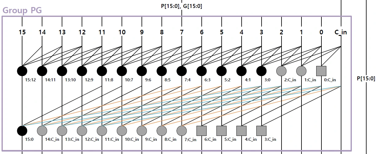
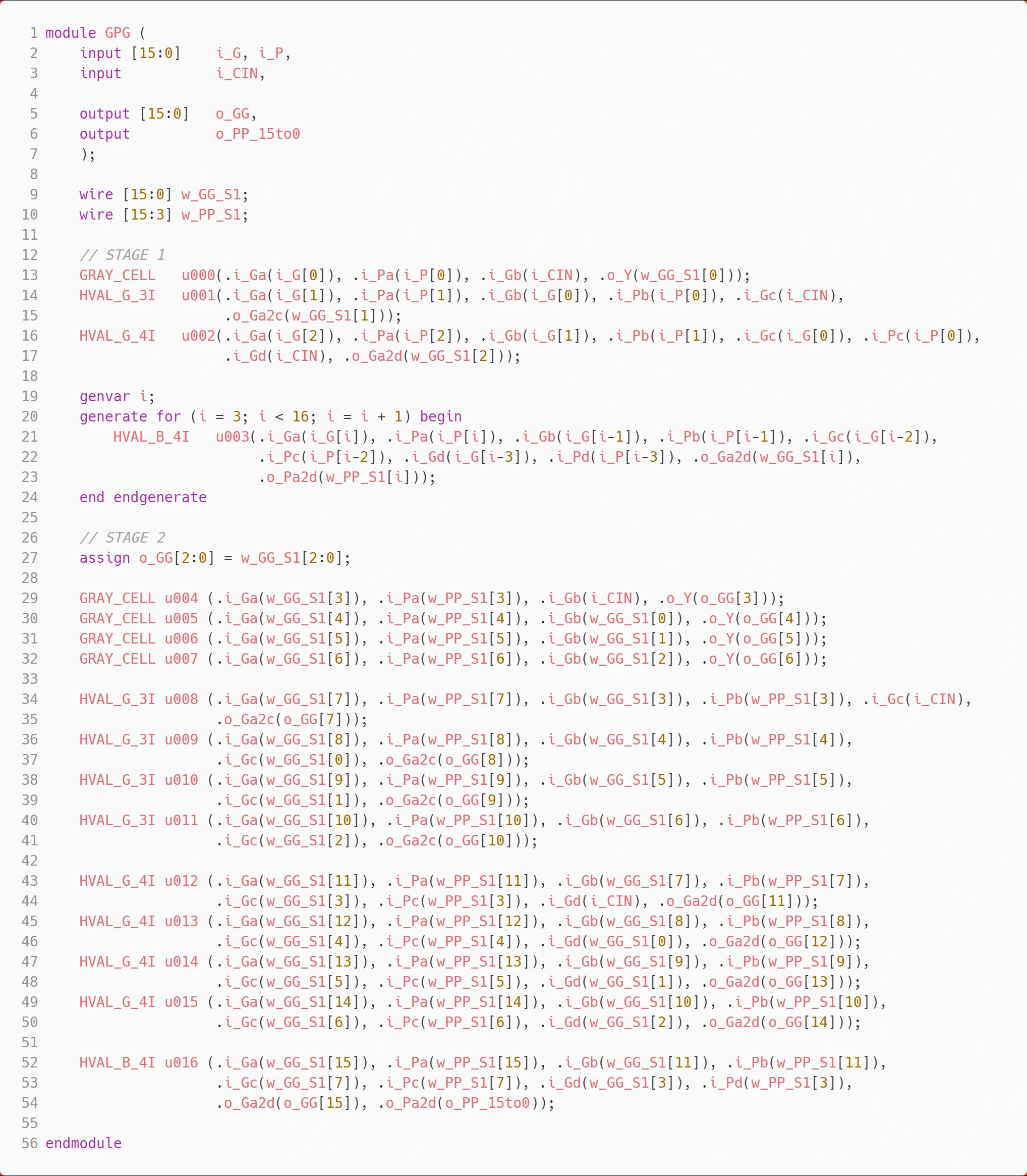
Figure 13 Group PG Logic
This logic performs the group PG operation on the P and G produced by the bitwise PG logic.
- 1 gray cell
- 1 3-higher valency gray cell
- 1 4-higher valency gray cell
- 13 4-higher valency black cells
- 4 gray cells
- 4 3-higher valency gray cells
- 4 4-higher valency gray cells
- 1 4-higher valency black cell
G15:0, which does not receive Cin here, is handled in the SUM logic with a gray cell.
SUM Logic
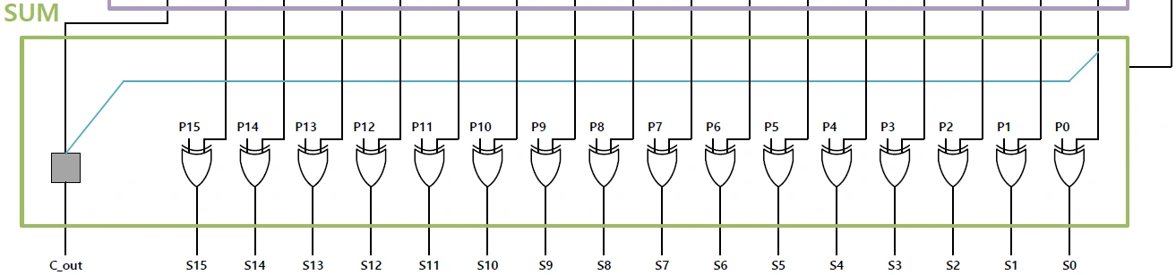
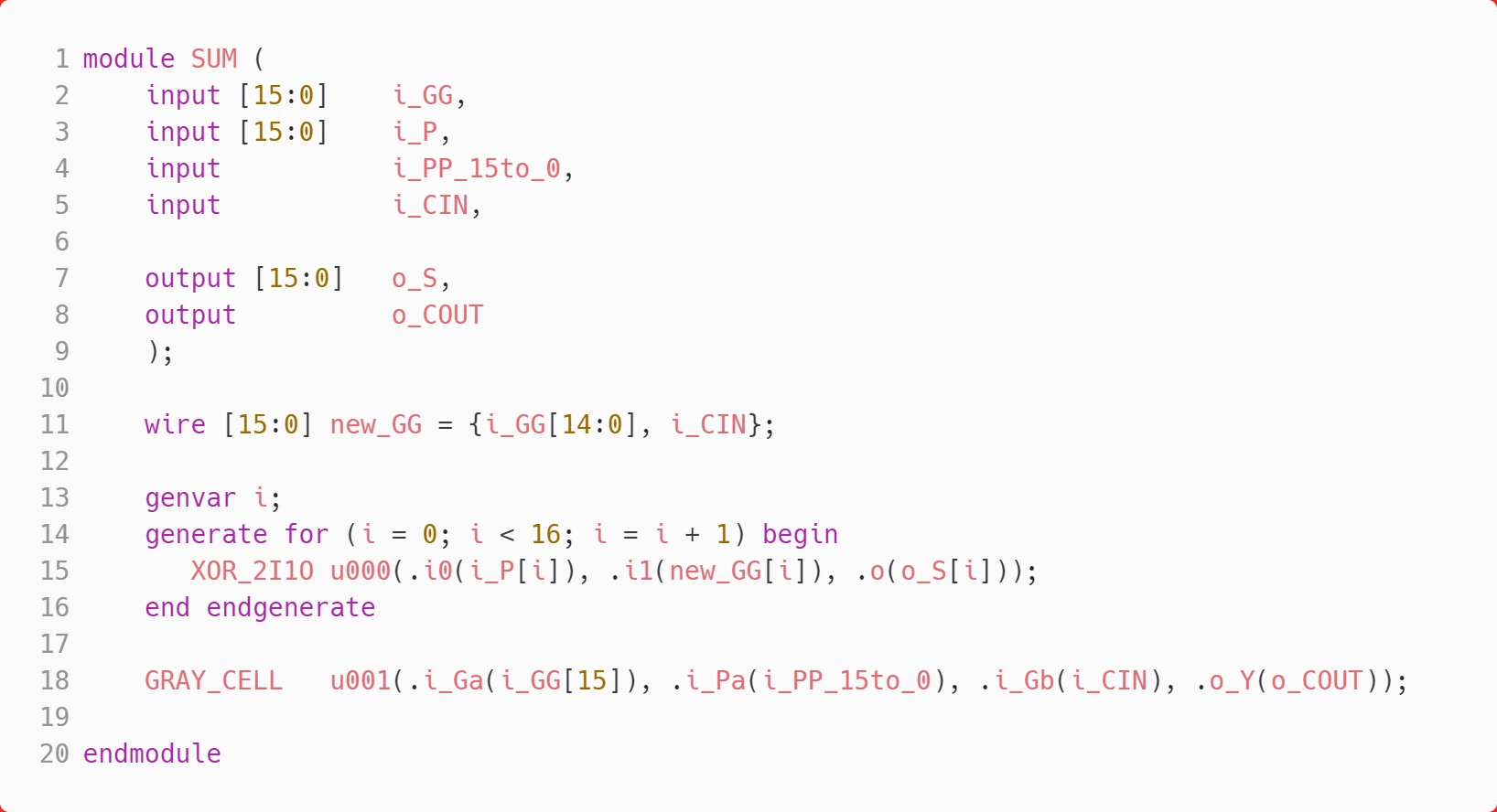
Figure 14 SUM Logic
This logic performs the final SUM operation on the P from the bitwise PG logic and the GG from the group PG logic. It performs XOR operations, and a gray cell combines G15:0 and P15:0 from the group PG logic with C_in to form G15:C_in, which becomes the final C_out.
The XOR's critical path goes through 3 NANDs, while the gray cell's critical path goes through 2 NANDs. Because of this, the critical path of the SUM logic does not pass through C_out.
4. Result Waveforms / Accuracy Verification
Test Bench
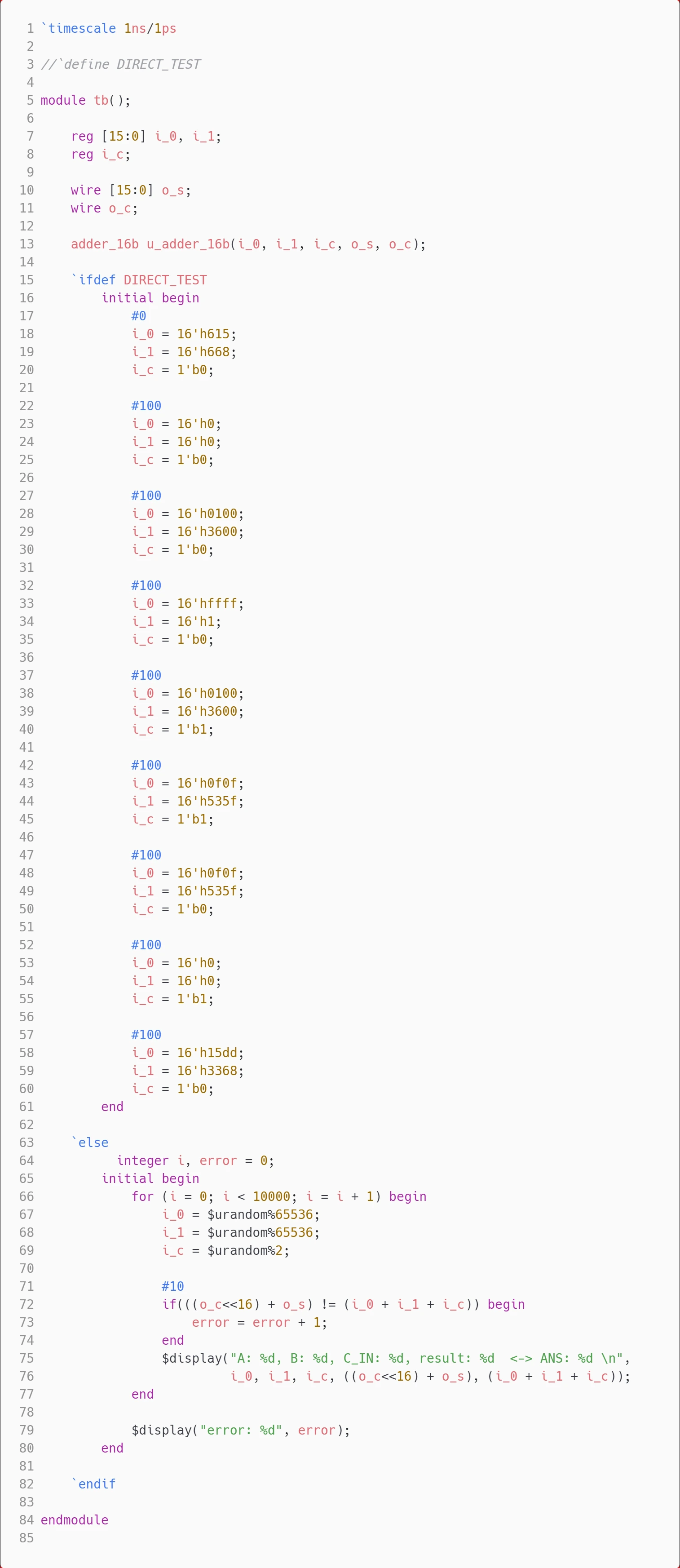
Figure 15 Test Bench
The testbench was designed to run in two modes. By default, it runs code that tests 10,000 random values. If you comment out the `define statement declared at the very top, you can simulate with values you enter manually. Below are the results for manually entered values with the `define statement commented out.
1) Result Waveforms
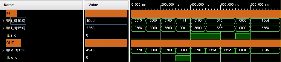
Figure 16 Result waveform in hex
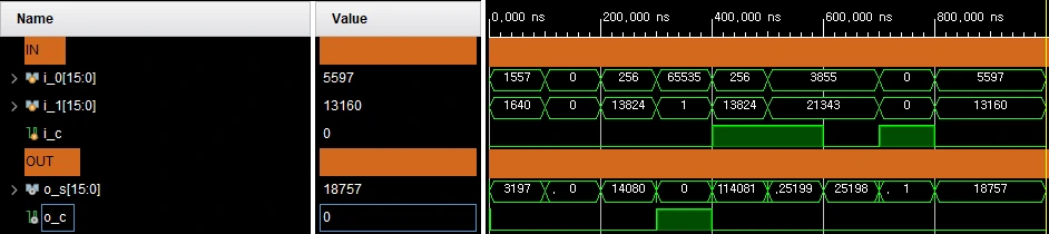
Figure 17 Result waveform in decimal
2) Accuracy Verification
To verify the accuracy of the module, I fed values into the inputs and checked whether the outputs were correct. Ideally I would verify every operation possible with 16-bit x 16-bit inputs, but that would mean 65536 x 65536 = 4,294,967,296 operations, including 0. Comparing all of them one by one in Vivado would also take a long time. So I verified with 10,000 randomly generated numbers instead.
These are the results of running the testbench code above with the `define statement declared. The code compares the output against the result of adding the random values and flags an error if they differ.
- $urandom%65536 // Generates a random value from 0 to 65535. 16 bits can represent values from 0 to 65535.
- ((o_c<<16) + o_s) // The carry is worth 65536, so shifting it and adding o_s gives the final value.

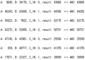
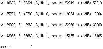
Figure 18 Results of 10,000 checks (partially omitted)
The verification confirmed that the adder works without problems. The error count is 0, so it operates correctly.
5. Performance Optimization / Performance Analysis
1) Performance Optimization
- Using higher-valency cells reduces logic levels, which cuts delay compared with chaining several gates
- In the Generate & Propagate cell, the AND gate is not used directly; it is taken from the middle of the XOR gate, saving gates
- The group PG logic computes 15:0 instead of 15:C_in and leaves the rest to the SUM logic, reducing logic levels
2) Performance Analysis
An adder's delay comes from the delay of each gate. The figure shows the critical path of the designed adder. Running a simulation to check it gives the results below.
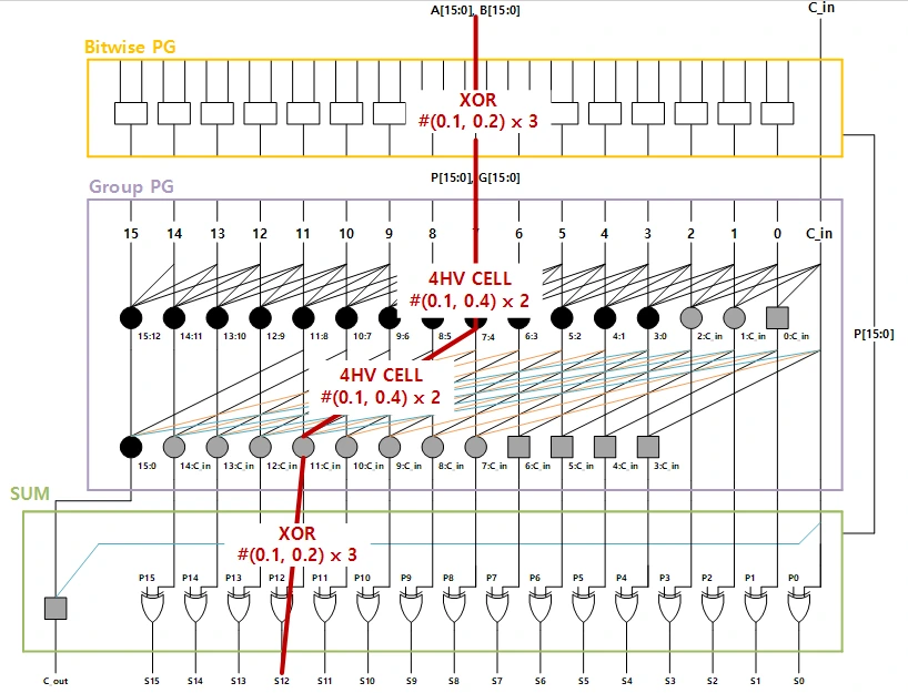
Figure 19 Critical Path
Kogge-Stone Adder using Higher Valency Cell
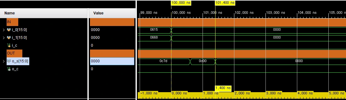
Original Kogge stone
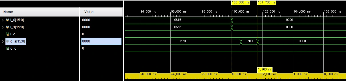
Figure 20 Result of 16'h0 + 16'h0
For 16'h0 + 16'h0 (C_in: 0), the original Kogge-Stone adder has a delay of 1700ns. The Kogge-Stone adder using higher-valency cells has a delay of 1400ns, confirming that the delay decreased.
Kogge-Stone Adder using Higher Valency Cell
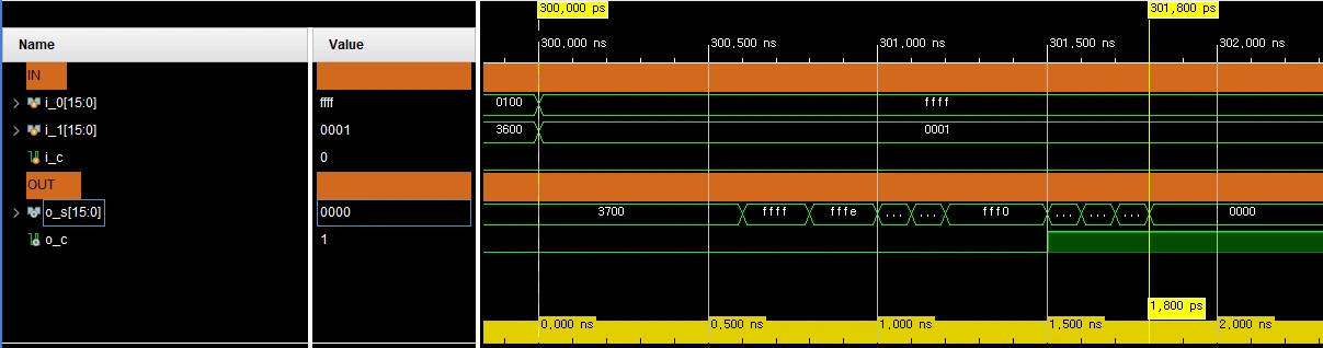
Original Kogge stone
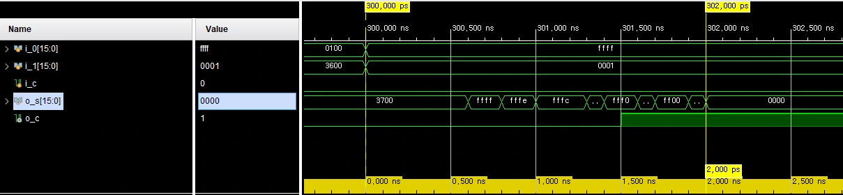
Figure 21 Result of 16'hffff + 16'h1
For 16'hffff + 16'h1 (C_in: 0), the original Kogge-Stone adder has a delay of 2000ns. The Kogge-Stone adder using higher-valency cells has a delay of 1800ns, confirming that the delay decreased.
6. An Alternative Design
This is an approach I came up with but did not actually implement. It is a sparse-tree adder in which the red blocks in the SUM logic are carry-lookahead adders. The red blocks compute at the same time as the group PG logic. Their outputs are then selected by the previous carry.
This design has the advantage of using less logic than the Kogge-Stone adder built only with higher-valency cells. In terms of performance, the red blocks are computed in parallel with the group PG logic, so they drop out, leaving only the XOR-based selection. That gives performance similar to the original Kogge-Stone adder built only with higher-valency cells.
Although it uses less logic than the Kogge-Stone adder built only with higher-valency cells, it could not improve performance, which was the goal of this project, so I only sketched it and did not implement it.
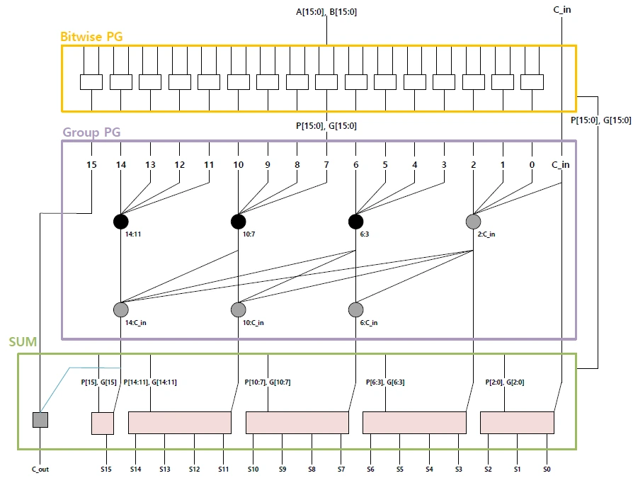
Figure 22 kogge stone sparse-tree adder using Higher Valency Cell