Chapter 2: Design Methodology Overview
Unlike traditional ASIC design, SoC (System-on-Chip) design depends on IP (Intellectual Property) reuse, the choice of design methodology, and where it sits on the spectrum from full-custom to programmable logic. This chapter summarizes the semiconductor circuit design process and SoC design methodologies.
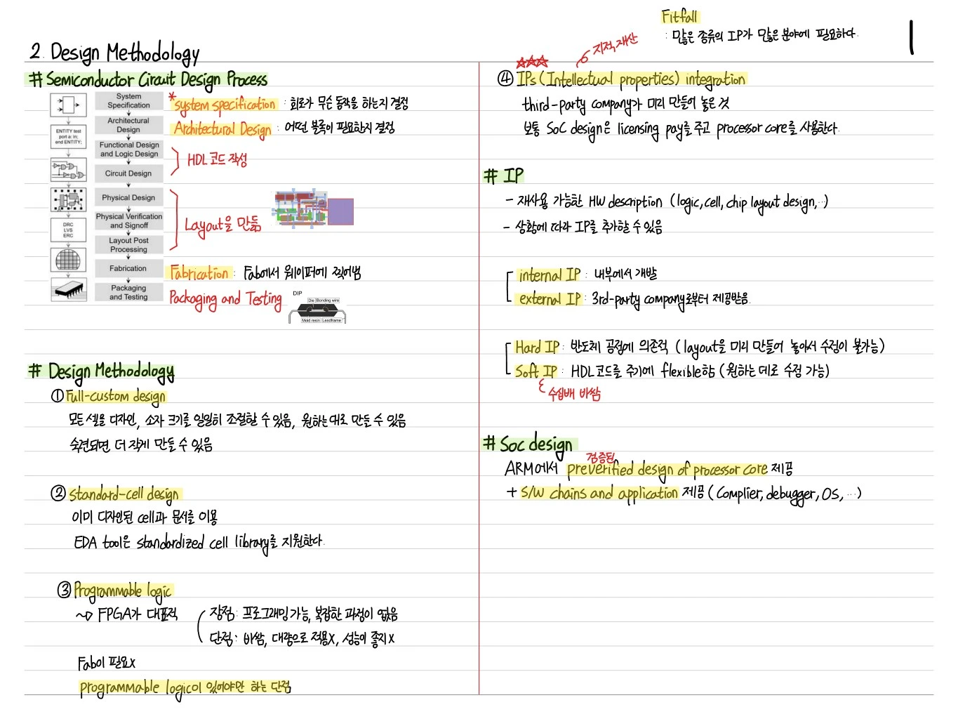
Semiconductor Circuit Design Process
Semiconductor circuit design proceeds through these steps:
- System Specification: define the requirements (what the chip should do)
- Architectural Design: architecture- and block-level decisions
- Functional Design and Logic Design: write HDL (Verilog/VHDL) code
- Circuit Design: transistor-level design
- Physical Design: decide the layout (area, placement)
- Physical Verification and Signoff: DRC, LVS, and STA checks
- Layout Post Processing: convert to GDSII
- Fabrication: wafers are manufactured at the fab
- Packaging and Testing: packaging and test
Design Methodology
① Full-Custom Design
- You can tune the placement and device size of every cell by hand (you can build exactly what you want)
- With skilled effort, you can build something better
- Optimal area/performance, but time and cost go way ↑
② Standard-Cell Design
- Uses predesigned cells as building blocks
- EDA tools support standardized cell libraries
- The most common ASIC design approach
③ Programmable Logic
- FPGAs are the typical example
- Pros: programmable, fast to get started
- Cons: expensive, not suited to high volume, lower area/performance than an ASIC
- No fab needed
- The drawback is that programmable logic leaves part of the silicon unused
Pitfall — Fields Where Much of the Design Starts from Existing IP
④ IPs (Intellectual Properties) Integration
- Using third-party components that are already built
- SoC designs usually license a processor core
IP (Intellectual Property)
- A reusable HW description (logic, cells, chip layout designs, etc.)
- Can also be added to a product as IP
Internal IP
- Developed in-house
External IP
- Supplied as a third-party component
Hard IP
- Depends on the process technology (the layout is already done, so it cannot be modified)
Soft IP
- Delivered as HDL code, so it is flexible (can be modified as needed)
SoC Design
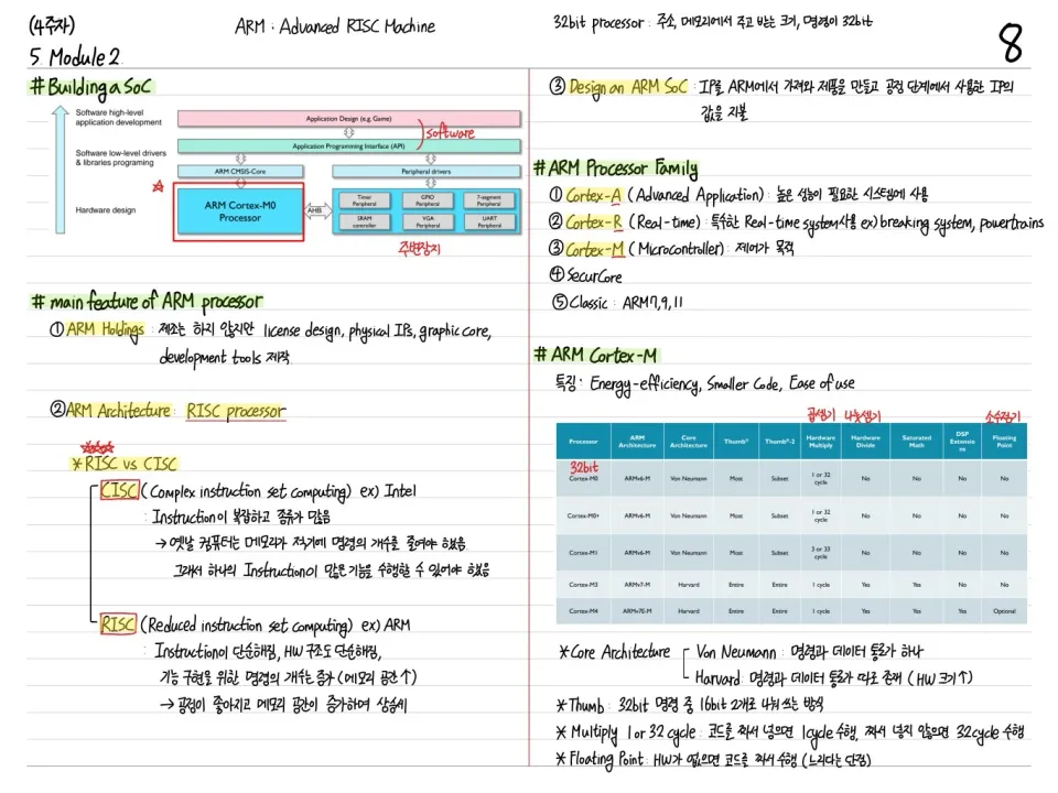
The vendor ARM provides a pre-verified design of the processor core + S/W chains and applications (compiler, debugger, OS, ...)
Summary
| Item | Description |
|---|---|
| Full-custom | Every device designed directly. Best area/performance. Cost ↑ |
| Standard-cell | Built from a cell library. The most common |
| Programmable (FPGA) | Fast verification. Lower area/performance |
| IP-based SoC | Third-party core (ARM Cortex, etc.) + in-house IP |
| Hard IP vs Soft IP | Fixed layout vs modifiable HDL |
The essence of SoC design is "how to reuse IP." ARM's Cortex series became the standard in the SoC market because it delivers well-verified soft IP + a compiler/OS stack in one package.