1. Topic
The Wallace tree multiplier is a structure for efficiently implementing a digital hardware circuit that multiplies two integers. It was invented in 1964 by Chris Wallace of Australia. The 8-bit multiplier I designed takes an 8-bit multiplier and an 8-bit multiplicand and returns a 16-bit product.
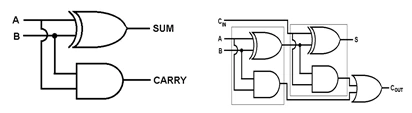
The design computes partial sums at each stage using half adders and full adders. A half adder takes 2 inputs and returns Sum and Carry as outputs. A full adder, in contrast, takes 3 inputs and returns Sum and Carry. Using these half adders and full adders, you can build a multiplier efficiently.
2. Design Flow
Below is the computation of the 8-bit Wallace multiplier. Groups of two use a half adder with 2 inputs, and groups of three use a full adder with 3 inputs.
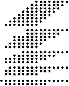
In the 8-bit Wallace multiplier, each dot in stage0 equals the AND of the corresponding bits of inputs A and B, position by position. In the code this is implemented as follows. p is an array of 8 entries, each 8 bits wide. It is easiest to read the number inside [ ] as the row number in stage0. For example, p[0] holds the bitwise AND of A and 8{B[0]}. 8{B[0]} repeats bit 0 of B eight times, because in stage0 only bit 0 of B takes part in the operation with A. In the nth stage, only bit n of B would be combined with A. Figure 3 shows which bit positions of a and b go into p as a result.
//p multiplied by A and B (and gate)
wire [7:0] p[7:0];
assign p[0] = A & {8{B[0]}};
assign p[1] = A & {8{B[1]}};
assign p[2] = A & {8{B[2]}};
assign p[3] = A & {8{B[3]}};
assign p[4] = A & {8{B[4]}};
assign p[5] = A & {8{B[5]}};
assign p[6] = A & {8{B[6]}};
assign p[7] = A & {8{B[7]}};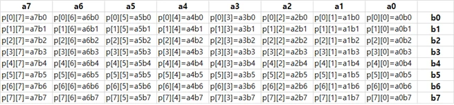
The values of p built this way are then computed by the half adders and full adders. The computation is shown below. Names start with 'f' for a full adder and 'h' for a half adder. The 's' or 'c' that follows stands for sum or carry, and the first digit is the stage number + 1. The number after that is the adder's unique ID.
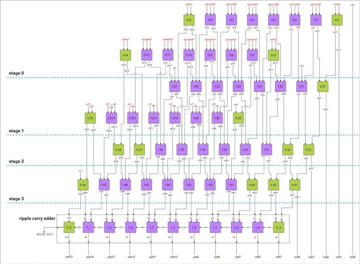
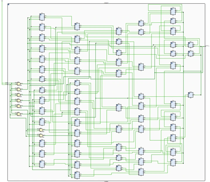 {: width="80%" height="80%"}
I implemented the testbench in two ways. Both take a and b as inputs and check whether the value computed with the ordinary multiplication operator matches the value computed by the Wallace tree.
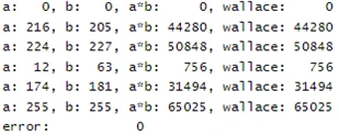
With tb1, all six inputs produced matching results. For example, with a = 224 and b = 227, the ordinary multiplication operator and the Wallace tree both gave 50848.
tb2 is a testbench that tries every possible input. It uses a nested for loop to feed every value into a and b. If the values differ, the error count increases by the number of mismatches. The simulation finished with 0 errors, which confirmed that the design was correct.
This design let me practice and apply Verilog syntax again and showed me where I was still lacking. It also helped me understand how to define modules, and finishing the design successfully gave me a sense of accomplishment. One regret is that I wanted to turn the final ripple carry adder into a module, but I could not handle the large number of inputs and did not manage to modularize it. I tried bundling the module inputs with the concatenation operator, but it failed. This looks like something I need to study further.
3. Test Bench
4. Code
module HA(sum, carry, a, b);

  output sum, carry;

    input a, b;


    xor (sum, a, b);

    and (carry, a, b);

endmodule


module FA(sum, carry, a, b, c);

    output sum, carry;

    input a, b, c;


    xor (sum, a, b, c);

    and (t1, a, b);

    xor (t2, a, b);

    and (t3, t2, c);

    or (carry, t1, t3);

endmodule

module multiplier(A,B,out);

    //inputs and outputs

    input [7:0] A,B;

    output [15:0] out;

    //connecting wire

    wire sh11, sh12, sh13, sh14, sh21, sh22, sh23, sh31, sh32, sh33, sh34, sh41, sh42, sh43, sh44;

    wire sf11, sf12, sf13, sf14, sf15, sf16, sf17, sf18, sf19, sf110, sf111, sf112;

    wire sf21, sf22, sf23, sf24, sf25, sf26, sf27, sf28, sf29, sf210, sf211, sf212, sf213;

    wire sf31, sf32, sf33, sf34, sf35, sf36;

    wire sf41, sf42, sf43, sf44, sf45, sf46, sf47;

    wire ch11, ch12, ch13, ch14, ch21, ch22, ch23, ch31, ch32, ch33, ch34, ch41, ch42, ch43, ch44;

    wire cf11, cf12, cf13, cf14, cf15, cf16, cf17, cf18, cf19, cf110, cf111, cf112;

    wire cf21, cf22, cf23, cf24, cf25, cf26, cf27, cf28, cf29, cf210, cf211, cf212, cf213;

     wire cf31, cf32, cf33, cf34, cf35, cf36;

     wire cf41, cf42, cf43, cf44, cf45, cf46, cf47;

   wire c0, c1, c2, c3, c4, c5, c6, c7, c8, c9, c10;


   //p multiplied by A and B (and gate)

    wire [7:0] p[7:0];

   assign  p[0] = A & {8{B[0]}};

   assign  p[1] = A & {8{B[1]}};

   assign  p[2] = A & {8{B[2]}};

   assign  p[3] = A & {8{B[3]}};

   assign  p[4] = A & {8{B[4]}};

   assign  p[5] = A & {8{B[5]}};

   assign  p[6] = A & {8{B[6]}};

   assign  p[7] = A & {8{B[7]}};


    // stage 0 _ first line

   assign out[0] = p[0][0];

   HA h11 (out[1], ch11, p[1][0], p[0][1]);

   FA f11 (sf11, cf11, p[2][0], p[1][1], p[0][2]);

     FA f12 (sf12, cf12, p[2][1], p[1][2], p[0][3]);

     FA f13 (sf13, cf13, p[2][2], p[1][3], p[0][4]);

     FA f14 (sf14, cf14, p[2][3], p[1][4], p[0][5]);

     FA f15 (sf15, cf15, p[2][4], p[1][5], p[0][6]);

     FA f16 (sf16, cf16, p[2][5], p[1][6], p[0][7]);

     HA h12 (sh12, ch12, p[2][6], p[1][7]);

    // stage 0 _ second line

     HA h13 (sh13, ch13, p[4][0], p[3][1]);

    FA f17 (sf17, cf17, p[5][0], p[4][1], p[3][2]);

    FA f18 (sf18, cf18, p[5][1], p[4][2], p[3][3]);

     FA f19 (sf19, cf19, p[5][2], p[4][3], p[3][4]);

     FA f110 (sf110, cf110, p[5][3], p[4][4], p[3][5]);

     FA f111 (sf111, cf111, p[5][4], p[4][5], p[3][6]);

     FA f112 (sf112, cf112, p[5][5], p[4][6], p[3][7]);

     HA h14 (sh14, ch14, p[5][6], p[4][7]);

    // stage 1 _ first line

     HA h21 (out[2], ch21, ch11, sf11);

     FA f21 (sf21, cf21, cf11, p[3][0], sf12);

     FA f22 (sf22, cf22, cf12, sf13, sh13);

     FA f23 (sf23, cf23, cf13, sf14, sf17);

     FA f24 (sf24, cf24, cf14, sf15, sf18);

     FA f25 (sf25, cf25, cf15, sf16, sf19);

     FA f26 (sf26, cf26, cf16, sh12, sf110);

     FA f27 (sf27, cf27, ch12, p[2][7], sf111);

    // stage 1 _ second line

    HA h22 (sh22, ch22, cf17, p[6][0]);

   FA f28 (sf28, cf28, cf18, p[6][1], p[7][0]);

   FA f29 (sf29, cf29, cf19, p[6][2], p[7][1]);

    FA f210 (sf210, cf210, cf110, p[6][3], p[7][2]);

    FA f211 (sf211, cf211, cf111, p[6][4], p[7][3]);

    FA f212 (sf212, cf212, cf112, p[6][5], p[7][4]);

    FA f213 (sf213, cf213, p[5][7], p[6][6], p[7][5]);

    HA h23 (sh23, ch23, p[6][7], p[7][6]);

    // stage 2

    HA h31 (out[3], ch31, ch21, sf21);

    HA h32 (sh32, ch32, cf21, sf22);

    FA f31 (sf31, cf31, cf22, ch13, sf23);

    FA f32 (sf32, cf32, cf23, sf24, sh22);

    FA f33 (sf33, cf33, cf24, sf25, sf28);

    FA f34 (sf34, cf34, cf25, sf26, sf29);

    FA f35 (sf35, cf35, cf26, sf27, sf210);

    FA f36 (sf36, cf36, cf27, sf112, sf211);

    HA h33 (sh33, ch33, sh14, sf212);

    HA h34 (sh34, ch34, ch14, sf213);

    // stage 3

    HA h41 (out[4], ch41, ch31, sh32);

    HA h42 (sh42, ch42, ch32, sf31);

    HA h43 (sh43, ch43, cf31, sf32);

    FA f41 (sf41, cf41, cf32, ch22, sf33);

    FA f42 (sf42, cf42, cf33, cf28, sf34);

    FA f43 (sf43, cf43, cf34, cf29, sf35);

    FA f44 (sf44, cf44, cf35, cf210, sf36);

    FA f45 (sf45, cf45, cf36, cf211, sh33);

    FA f46 (sf46, cf46, ch33, cf212, sh34);

    FA f47 (sf47, cf47, ch34, cf213, sh23);

    HA h44 (sh44, ch44, ch23, p[7][7]);

    // stage 4 ripple carry adder

    HA h_a (out[5], c0, ch41, sh42);

     FA f_a (out[6], c1, c0, ch42, sh43);

   FA f_b (out[7], c2, c1, ch43, sf41);

    FA f_c (out[8], c3, c2, cf41, sf42);

   FA f_d (out[9], c4, c3, cf42, sf43);

   FA f_e (out[10], c5, c4, cf43, sf44);

     FA f_f (out[11], c6, c5, cf44, sf45);

    FA f_g (out[12], c7, c6, cf45, sf46);

     FA f_h (out[13], c8, c7, cf46, sf47);

     FA f_i (out[14], c9, c8, cf47, sh44);

   HA h_b (out[15], c10, c9, ch44);


endmodule


module tb;


  reg [7:0] a, b;

  wire [15:0] mout;


  multiplier m1 (a, b, mout);

  wire [15:0] test;

  assign test = a * b;


  initial

  begin

     a = 4'd0;  b=4'd0;

  #1 a = 4'd0;  b=4'd1;

  #1 a = 4'd7;  b=4'd5;

  #1 a = 4'd10; b=4'd10;

  #1 a = 4'd15; b=4'd15;

  #1 a = 4'd13; b=4'd12;


  end

  initial

  begin

    $monitor("a*b: %d, wallace: %d", test, mout);

    $dumpfile("dump.vcd"); $dumpvars;

  end

endmodule